JAJSG06E April   2016  – October 2018 LMG3410R070 , LMG3411R070

PRODUCTION DATA.  

  1. 特長
  2. アプリケーション
  3. 概要
    1.     Device Images
      1.      ブロック概略図
      2.      100V/nsを超えるスイッチング性能
  4. 改訂履歴
  5. 概要(続き)
  6. Pin Configuration and Functions
    1.     Pin Functions
  7. Specifications
    1. 7.1 Absolute Maximum Ratings
    2. 7.2 ESD Ratings
    3. 7.3 Recommended Operating Conditions
    4. 7.4 Thermal Information
    5. 7.5 Electrical Characteristics
    6. 7.6 Switching Characteristics
    7. 7.7 Typical Characteristics
  8. Parameter Measurement Information
    1. 8.1 Switching Parameters
      1. 8.1.1 Turn-on Delays
      2. 8.1.2 Turn-off Delays
      3. 8.1.3 Drain Slew Rate
      4. 8.1.4 Turn-on and Turn-off Energy
  9. Detailed Description
    1. 9.1 Overview
    2. 9.2 Functional Block Diagram
    3. 9.3 Feature Description
      1. 9.3.1 Direct-Drive GaN Architecture
      2. 9.3.2 Internal Buck-Boost DC-DC Converter
      3. 9.3.3 Internal Auxiliary LDO
      4. 9.3.4 Fault Detection
        1. 9.3.4.1 Over-current Protection
        2. 9.3.4.2 Over-Temperature Protection and UVLO
      5. 9.3.5 Drive Strength Adjustment
    4. 9.4 Device Functional Modes
      1. 9.4.1 Low-Power Mode
  10. 10Application and Implementation
    1. 10.1 Application Information
    2. 10.2 Typical Application
      1. 10.2.1 Design Requirements
      2. 10.2.2 Detailed Design Procedure
        1. 10.2.2.1 Slew Rate Selection
          1. 10.2.2.1.1 Startup and Slew Rate with Bootstrap High-Side Supply
        2. 10.2.2.2 Signal Level-Shifting
        3. 10.2.2.3 Buck-Boost Converter Design
      3. 10.2.3 Application Curves
    3. 10.3 Paralleling GaN Devices
    4. 10.4 Do's and Don'ts
  11. 11Power Supply Recommendations
    1. 11.1 Using an Isolated Power Supply
    2. 11.2 Using a Bootstrap Diode
      1. 11.2.1 Diode Selection
      2. 11.2.2 Managing the Bootstrap Voltage
      3. 11.2.3 Reliable Bootstrap Start-up
  12. 12Layout
    1. 12.1 Layout Guidelines
      1. 12.1.1 Power Loop Inductance
      2. 12.1.2 Signal Ground Connection
      3. 12.1.3 Bypass Capacitors
      4. 12.1.4 Switch-Node Capacitance
      5. 12.1.5 Signal Integrity
      6. 12.1.6 High-Voltage Spacing
      7. 12.1.7 Thermal Recommendations
    2. 12.2 Layout Example
  13. 13デバイスおよびドキュメントのサポート
    1. 13.1 デバイス・サポート
      1. 13.1.1 デベロッパー・ネットワークの製品に関する免責事項
    2. 13.2 ドキュメントのサポート
      1. 13.2.1 関連資料
    3. 13.3 ドキュメントの更新通知を受け取る方法
    4. 13.4 コミュニティ・リソース
    5. 13.5 商標
    6. 13.6 静電気放電に関する注意事項
    7. 13.7 Glossary
  14. 14メカニカル、パッケージ、および注文情報

Switching Parameters

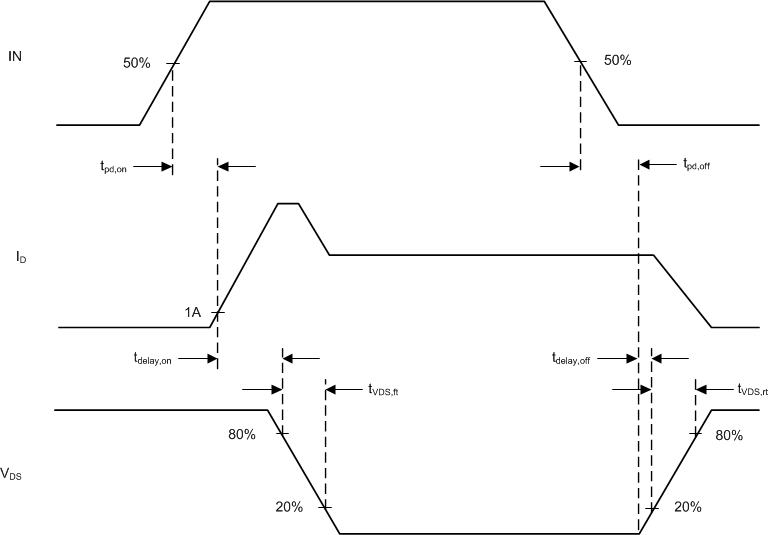
The circuit used to measure most switching parameters is shown in Figure 11. The top LMG341xR070 in this circuit is used to re-circulate the inductor current and functions in third-quadrant mode only. The bottom device is the active device; it is turned on to increase the inductor current to the desired test current. The bottom device is then turned off and on to create switching waveforms at a specific inductor current. Both the drain current (at the source) and the drain-source voltage is measured. The specific timing measurement is shown in Figure 12. It is recommended to use the half-bridge as double pulse tester. Excessive 3rd quadrant operation may over heat the top LMG341xR070.
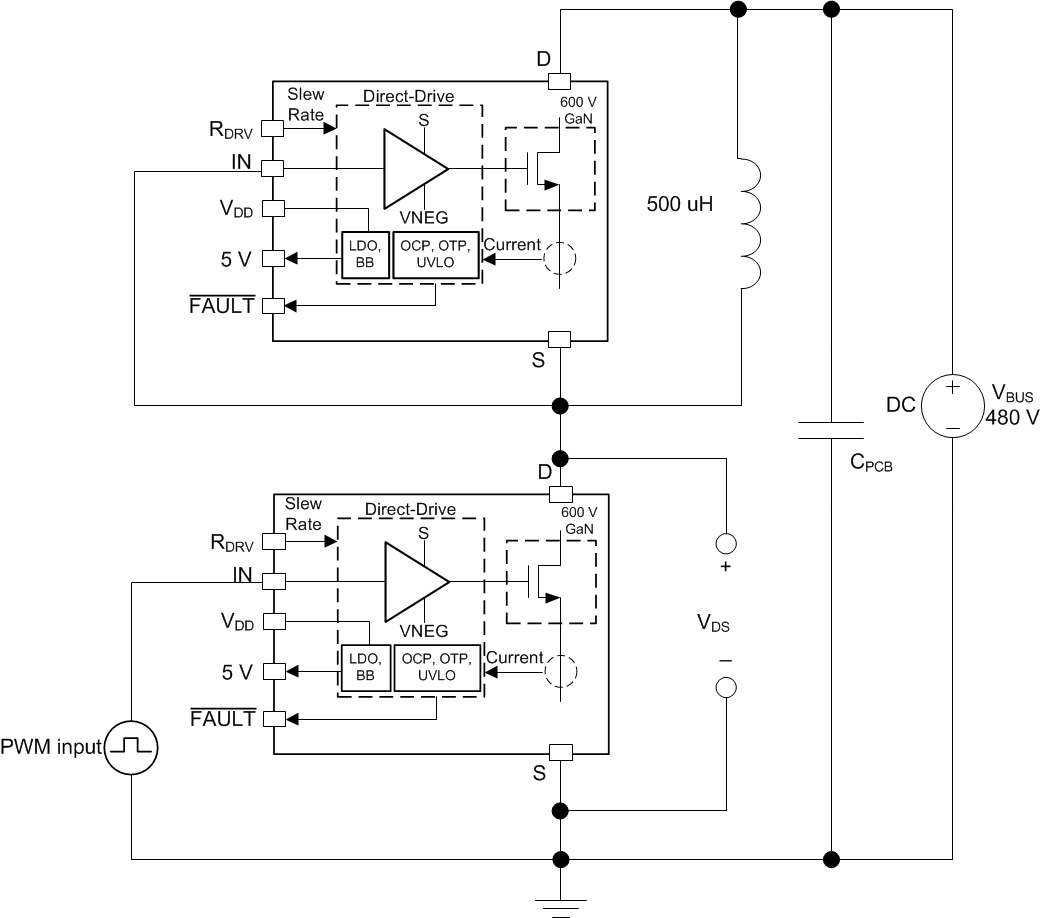
LMG3410R070 LMG3411R070 LMG3410R070-switching-test-diagram-SNOSD10.gifFigure 11. Circuit Used to Determine Switching Parameters
LMG3410R070 LMG3411R070 LMG3410R070-measurement-to-determine-prop-delay-and-slew-rate-SNOSD10.gifFigure 12. Measurement to Determine Propagation Delays and Slew Rates