JAJSG07E August   2012  – August 2018 LMZ21701

PRODUCTION DATA.  

  1. 特長
  2. アプリケーション
  3. 概要
    1.     Device Images
      1.      概略回路図
      2.      VIN = 12Vでの効率
  4. 改訂履歴
  5. Pin Configuration and Functions
    1.     Pin Functions
  6. Specifications
    1. 6.1 Absolute Maximum Ratings
    2. 6.2 ESD Ratings
    3. 6.3 Recommended Operating Conditions
    4. 6.4 Thermal Information
    5. 6.5 Electrical Characteristics
    6. 6.6 Typical Characteristics
  7. Detailed Description
    1. 7.1 Overview
    2. 7.2 Functional Block Diagram
    3. 7.3 Package Construction
    4. 7.4 Feature Description
      1. 7.4.1 Input Undervoltage Lockout
      2. 7.4.2 Enable Input (EN)
      3. 7.4.3 Soft Start and Tracking Function (SS)
      4. 7.4.4 Power Good Function (PG)
      5. 7.4.5 Output Voltage Setting
      6. 7.4.6 Output Current Limit and Output Short Circuit Protection
      7. 7.4.7 Thermal Protection
    5. 7.5 Device Functional Modes
      1. 7.5.1 PWM Mode Operation
      2. 7.5.2 PSM Operation
  8. Application and Implementation
    1. 8.1 Application Information
    2. 8.2 Typical Application
      1. 8.2.1 Design Requirements
      2. 8.2.2 Detailed Design Procedure
        1. 8.2.2.1 Custom Design With WEBENCH® Tools
        2. 8.2.2.2 Input Capacitor (CIN)
        3. 8.2.2.3 Output Capacitor (COUT)
        4. 8.2.2.4 Soft-start Capacitor (CSS)
        5. 8.2.2.5 Power Good Resistor (RPG)
        6. 8.2.2.6 Feedback Resistors (RFBB and RFBT)
      3. 8.2.3 Application Curves
        1. 8.2.3.1 VOUT = 1.2 V
        2. 8.2.3.2 VOUT = 1.8 V
        3. 8.2.3.3 VOUT = 2.5 V
        4. 8.2.3.4 VOUT = 3.3 V
        5. 8.2.3.5 VOUT = 5.0 V
    3. 8.3 Do's and Don'ts
  9. Power Supply Recommendations
    1. 9.1 Voltage Range
    2. 9.2 Current Capability
    3. 9.3 Input Connection
      1. 9.3.1 Voltage Drops
      2. 9.3.2 Stability
  10. 10Layout
    1. 10.1 Layout Guidelines
      1. 10.1.1 Minimize the High di/dt Loop Area
      2. 10.1.2 Protect the Sensitive Nodes in the Circuit
      3. 10.1.3 Provide Thermal Path and Shielding
    2. 10.2 Layout Example
      1. 10.2.1 High Density Layout Example for Space Constrained Applications
        1. 10.2.1.1 35 mm² Solution Size (Single Sided)
  11. 11デバイスおよびドキュメントのサポート
    1. 11.1 デバイス・サポート
      1. 11.1.1 開発サポート
        1. 11.1.1.1 WEBENCH®ツールによるカスタム設計
    2. 11.2 商標
    3. 11.3 静電気放電に関する注意事項
    4. 11.4 Glossary
  12. 12メカニカル、パッケージ、および注文情報
    1. 12.1 Tape and Reel Information

VOUT = 1.2 V

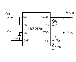
LMZ21701 TYP_SCH.gifFigure 20. Typical Applications Circuit
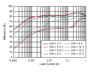
LMZ21701 D013_LMZ21701_25C_1.2VOUT_EFFICIENCY_LOG_SNVS853.gifFigure 22. Efficiency VOUT = 1.2 V
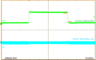
LMZ21701 LMZ21701_1.2VOUT_LOAD_TRANS_100mA_to_1000mA_snvs853.gifFigure 24. Load Transient VOUT = 1.2 V
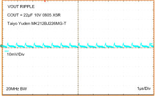
LMZ21701 LMZ21701_1.2VOUT_RIPPLE_20MHzBW_snvs853.gifFigure 26. 20 MHz Oscilloscope Bandwidth
Output Voltage Ripple VOUT = 1.2 V
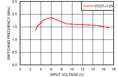
LMZ21701 LMZ21701_FSW_1.2VOUT_snvs853.pngFigure 28. Typical Switching Frequency at 1000 mA Load VOUT = 1.2 V
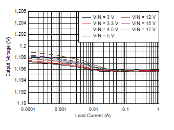
LMZ21701 D014_LMZ21701_25C_1.2VOUT_LINE_AND_LOAD_REG_LOG_SNVS853.gifFigure 30. Line and Load Regulation VOUT = 1.2 V
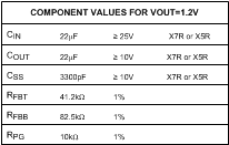
LMZ21701 1.2V_BOM_snvs853.gifFigure 21. External Component Values
(VOUT = 1.2 V)
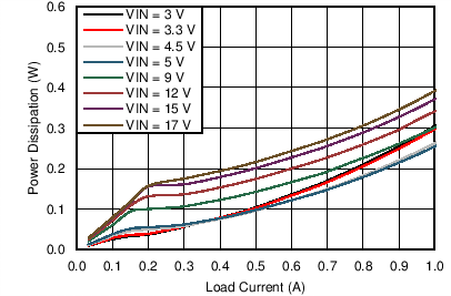
LMZ21701 LMZ21701_25C_1.2VOUT_POWER_DISSIPATION_snvs853.pngFigure 23. Power Dissipation VOUT = 1.2 V
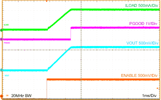
LMZ21701 LMZ21701_1.2VOUT_STARTUP_snvs853.gifFigure 25. Startup VOUT = 1.2 V
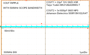
LMZ21701 LMZ21701_1.2VOUT_RIPPLE_500MHzBW_snvs853.gifFigure 27. 500 MHz Oscilloscope Bandwidth, 3x1000 pF additional output capacitance
Output Voltage Ripple and HF Noise VOUT = 1.2 V
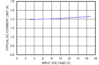
LMZ21701 LMZ21701_ICL_1.2V_85C_snvs853.pngFigure 29. Typical Current Limit VOUT = 1.2 V, TA = 85 °C
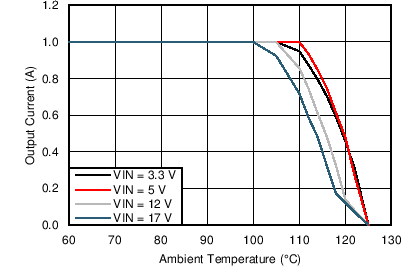
LMZ21701 LMZ21701SIL_1.2VO_47CperW_snvs853.pngFigure 31. Thermal Derating for θJA = 47 ºC/W, VOUT = 1.2 V