JAJSH37A August 2019 – August 2019 TPS56C230
PRODUCTION DATA.
- 1 特長
- 2 アプリケーション
- 3 概要
- 4 改訂履歴
- 5 概要(続き)
- 6 Pin Configuration and Functions
- 7 Specifications
- 8 Detailed Description
- 9 Application and Implementation
- 10Power Supply Recommendations
- 11Layout
- 12デバイスおよびドキュメントのサポート
- 13メカニカル、パッケージ、および注文情報
6 Pin Configuration and Functions
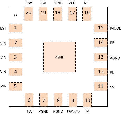
RJE Package
20-Pin VQFN
Top View

Pin Functions
| PIN | I/O | DESCRIPTION | |
|---|---|---|---|
| NAME | NO. | ||
| BST | 1 | I | Supply input for the gate drive voltage of the high-side MOSFET. Connect the bootstrap capacitor between BST and SW, 0.1 uF is recommended. |
| VIN | 2,3,4,5 | P | Input voltage supply pin for the control circuitry. Connect the input decoupling capacitors between VIN and PGND. |
| SW | 6,19,20 | O | Switching node connection to the inductor and bootstrap capacitor for buck. This pin voltage swings from a diode voltage below the ground up to input voltage of buck. |
| PGND | 7,8,18,Pad | G | Power GND terminal for the controller circuit and the internal circuitry. |
| PGOOD | 9 | O | Open drain power good indicator. It is asserted low if output voltage is out of PG threshold, over voltage or if the device is under thermal shutdown, EN shutdown or during soft start. |
| SS | 11 | I | Soft-Start time selection pin. Connecting an external capacitor sets the soft-start time and if no external capacitor is connected, the soft-start time is about 1.2ms. |
| NC | 10,16 | Not connect. Can be connected to GND plane for better thermal achieved. | |
| EN | 12 | I | Enable input of buck converter |
| AGND | 13 | G | Ground of internal analog circuitry. Connect AGND to GND plane with a short trace. |
| FB | 14 | I | Feedback sensing pin for Buck output voltage. Connect this pin to the resistor divider between output voltage and AGND. |
| MODE | 15 | I | Light load operation mode selection pin. Connect this pin to a resistor divider from VCC and AGND for different MODE options shown in Table 1 |
| VCC | 17 | O | The driver and control circuits are powered from this voltage. Decouple with a minimum 1 μF ceramic capacitor as close to VCC as possible. |