JAJSHF6A May   2019  – August 2020 TMP390

PRODUCTION DATA  

  1. 特長
  2. アプリケーション
  3. 概要
  4. Revision History
  5. Pin Configuration and Functions
    1.     Pin Functions
  6. Specifications
    1. 6.1 Absolute Maximum Ratings
    2. 6.2 ESD Ratings
    3. 6.3 Recommended Operating Conditions
    4. 6.4 Thermal Information
    5. 6.5 Electrical Characteristics
    6. 6.6 Typical Characteristics
  7. Detailed Description
    1. 7.1 Overview
    2. 7.2 Functional Block Diagram
    3. 7.3 Feature Description
      1. 7.3.1 TMP390 Programming Tables
      2. 7.3.2 Trip Test
      3. 7.3.3 20°C Hysteresis
    4. 7.4 Device Functional Modes
  8. Application and Implementation
    1. 8.1 Applications Information
    2. 8.2 Typical Applications
      1. 8.2.1 Simplified Application Schematic
        1. 8.2.1.1 Design Requirements
        2. 8.2.1.2 Detailed Design Procedure
        3. 8.2.1.3 Application Curves
      2. 8.2.2 TMP390 With 10°C Hysteresis
        1. 8.2.2.1 Design Requirements
        2. 8.2.2.2 Detailed Design Procedure
        3. 8.2.2.3 Application Curve
      3. 8.2.3 One Channel Operation for Hot Trip Point up to 124°C
        1. 8.2.3.1 Application Curve
      4. 8.2.4 One Channel Operation for Cold Trip Point
        1. 8.2.4.1 Application Curve
  9. Power Supply Recommendations
  10. 10Layout
    1. 10.1 Layout Guidelines
    2. 10.2 Layout Example
  11. 11Device and Documentation Support
    1. 11.1 ドキュメントの更新通知を受け取る方法
    2. 11.2 サポート・リソース
    3. 11.3 Trademarks
    4. 11.4 Electrostatic Discharge Caution
    5. 11.5 用語集
  12. 12Mechanical, Packaging, and Orderable Information

One Channel Operation for Cold Trip Point

Figure 8-7 shows the TMP390 configured for one channel operation, with a single resistor to set the warm trip point and hysteresis. The resistor values for one channel warm trip point is same as described in Table 7-2.
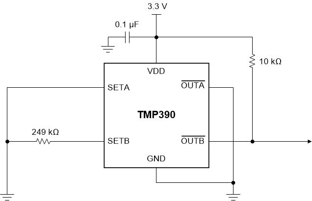
GUID-373C892D-CFE0-46AD-B00D-DB7C5A548306-low.gifFigure 8-7 TMP390 One Channel (Cold) Operation Example Circuit With –20°C Trip Point and 10°C Hysteresis