JAJSJ14 August   2020 TPS25980

PRODUCTION DATA  

  1. 特長
  2. アプリケーション
  3. 概要
  4. Revision History
  5. Device Comparison Table
  6. Pin Configuration and Functions
    1.     7
  7. Specifications
    1. 7.1 Absolute Maximum Ratings
    2. 7.2 ESD Ratings
    3. 7.3 Recommended Operating Conditions
    4. 7.4 Thermal Information
    5. 7.5 Electrical Characteristics
    6. 7.6 Timing Requirements
    7. 7.7 Switching Characteristics
    8. 7.8 Typical Characteristics
  8. Detailed Description
    1. 8.1 Overview
    2. 8.2 Functional Block Diagram
    3. 8.3 Feature Description
      1. 8.3.1 Undervoltage Protection (UVLO and UVP)
      2. 8.3.2 Overvoltage Protection (OVP)
      3. 8.3.3 Inrush Current, Overcurrent, and Short-Circuit Protection
        1. 8.3.3.1 Slew Rate and Inrush Current Control (dVdt)
        2. 8.3.3.2 Circuit Breaker
        3. 8.3.3.3 Short-Circuit Protection
      4. 8.3.4 Overtemperature Protection (OTP)
      5. 8.3.5 Analog Load Current Monitor (IMON)
      6. 8.3.6 Power Good (PG)
      7. 8.3.7 Load Detect/Handshake (LDSTRT)
    4. 8.4 Fault Response
    5. 8.5 Device Functional Modes
  9. Application and Implementation
    1. 9.1 Application Information
    2. 9.2 Typical Application: Patient Monitoring System in Medical Applications
      1. 9.2.1 Design Requirements
      2. 9.2.2 Detailed Design Procedure
        1. 9.2.2.1 Device Selection
        2. 9.2.2.2 Setting the Current Limit Threshold: RILIM Selection
        3. 9.2.2.3 Setting the Undervoltage Lockout Set Point
        4. 9.2.2.4 Choosing the Current Monitoring Resistor: RIMON
        5. 9.2.2.5 Setting the Output Voltage Ramp Time (TdVdt)
          1. 9.2.2.5.1 Case 1: Start-Up Without Load: Only Output Capacitance COUT Draws Current
          2. 9.2.2.5.2 Case 2: Start-Up With Load: Output Capacitance COUT and Load Draw Current
        6. 9.2.2.6 Setting the Load Handshake (LDSTRT) Delay
        7. 9.2.2.7 Setting the Transient Overcurrent Blanking Interval (tITIMER)
        8. 9.2.2.8 Setting the Auto-Retry Delay and Number of Retries
      3. 9.2.3 Application Curves
    3. 9.3 System Examples
      1. 9.3.1 Optical Module Power Rail Path Protection
        1. 9.3.1.1 Design Requirements
        2. 9.3.1.2 Device Selection
        3. 9.3.1.3 External Component Settings
        4. 9.3.1.4 Voltage Drop
        5. 9.3.1.5 Application Curves
      2. 9.3.2 Input Protection for 12-V Rail Applications: PCIe Cards, Storage Interfaces and DC Fans
  10. 10Power Supply Recommendations
    1. 10.1 Transient Protection
    2. 10.2 Output Short-Circuit Measurements
  11. 11Layout
    1. 11.1 Layout Guidelines
    2. 11.2 Layout Example
  12. 12Device and Documentation Support
    1. 12.1 Documentation Support
      1. 12.1.1 Related Documentation
        1. 12.1.1.1 Related Links
    2. 12.2 Receiving Notification of Documentation Updates
    3. 12.3 Support Resources
    4. 12.4 Trademarks
    5. 12.5 静電気放電に関する注意事項
    6. 12.6 Glossary
  13. 13Mechanical, Packaging, and Orderable Information

Typical Characteristics

GUID-F0CE9BDA-0601-4D6C-8966-761320DF2687-low.gifFigure 7-1 Supply UVP Threshold vs Temperature
GUID-E06CD06A-EB22-4E3A-90BA-33E43E5FFB07-low.gif
TPS259803x Variants
Figure 7-3 Supply OVP Threshold vs Temperature
GUID-3F4EDA36-A686-449E-A0AF-DAFED16B8110-low.gifFigure 7-5 EN/UVLO Threshold vs Temperature
GUID-D39EE16F-630D-4911-917E-F71288F2F2BF-low.gifFigure 7-7 EN/UVLO Falling Threshold for Lowest Current Consumption
GUID-5F82869B-6C98-49A0-8D38-28238E5EEEA4-low.gif
VENUVLO = 0 V, OUT = Open
Figure 7-9 Deep Shut-Down Current vs Temperature
GUID-20200807-CA0I-PKGC-WF1R-NPH7Q3THNDBM-low.gif
Across Process, Voltage, Temperature Corners
Figure 7-11 Output Current Limit (ILIM) Accuracy
GUID-43E76963-7FCD-4415-AF53-53AC5F453A43-low.gifFigure 7-13 ITIMER Voltage Threshold Delta vs Temperature
GUID-35A825EA-5409-43D6-827C-596B7117CEBB-low.gifFigure 7-15 LDSTRT Charging Current vs Temperature
GUID-5374A88D-A13F-44E3-A8E8-34D2F0329A9A-low.gifFigure 7-17 DVDT Charging Current vs Temperature
GUID-EE354442-16FB-4C9F-8EA8-51C0D6C3EBCF-low.gifFigure 7-19 RETRY_DLY Oscillator Hysteresis vs Temperature
GUID-1BBB6971-0512-4D6D-975B-7F431D5C8563-low.gifFigure 7-21 NRETRY Oscillator Hysteresis vs Temperature
GUID-20200807-CA0I-SPTQ-FJ86-HSDJGCVFC7H9-low.gifFigure 7-23 Thermal Shutdown Plot - Inrush/Overload
GUID-38144B3E-8BEF-4FCB-8EB4-093D5E4949A0-low.gif
TPS259802x Variants
Figure 7-2 Supply OVP Threshold vs Temperature
GUID-E16BE2CF-7980-4D2F-B5E9-48F345BCD9D4-low.gif
TPS259804x Variants
Figure 7-4 Supply OVP Threshold vs Temperature
GUID-97BD138F-D11C-4DD4-B675-D674B256DAD2-low.gif
VENUVLO = 2 V, OUT = Open
Figure 7-6 Quiescent Current vs Temperature
GUID-74891332-EB9D-4254-B898-0E462E529AD9-low.gif
VENUVLO = 1 V, OUT = Open
Figure 7-8 Shut-Down Current vs Temperature
GUID-20200807-CA0I-CQDS-NHZM-VKWSCBLC5TMR-low.gifFigure 7-10 Output Current Limit (ILIM) vs RILIM
GUID-95F38492-E083-4C61-99DA-86050D851176-low.gif
VIN = 0 V
Figure 7-12 Power Good Output Voltage (De-asserted State) vs Temperature
GUID-8F896EA6-A5AE-4E93-AB0B-B04A683047AA-low.gifFigure 7-14 ITIMER Discharge Current vs Temperature
GUID-7355F6C2-134B-4BD2-8954-6E81FA9134DC-low.gifFigure 7-16 LDSTRT Threshold Voltage vs Temperature
GUID-75F6C9C2-086E-4B42-A696-79A1E1827318-low.gifFigure 7-18 RETRY_DLY Bias Current vs Temperature
GUID-A89ED319-7DF4-4A04-A3A7-C61CC08B5CF5-low.gifFigure 7-20 NRETRY Bias Current vs Temperature
GUID-D9854117-01A7-4903-AA05-9ED8C69567F6-low.gifFigure 7-22 Thermal Shutdown Plot - Steady State
GUID-CC3D805D-3642-4F58-82FA-F7E01E18C9B6-low.png
CIN = 1 μF COUT = 220 μF CdVdt = 3.3 nF
Figure 7-24 Hotplug
GUID-299A2F56-D6AB-4222-B3C4-B328EDE80786-low.png
COUT = 220 μF CdVdt = 3.3 nF ROUT = 6 Ω
Figure 7-26 Startup With EN Into Resistive Load - dVdt Limited
GUID-20200807-CA0I-XQTZ-G9Z0-16WWRX2N7DK7-low.gif
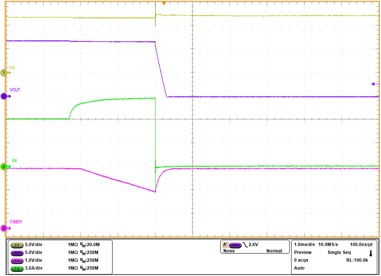
RILIM = 182 Ω CITIMER = 4.7 nF
Figure 7-28 Circuit Breaker With Transient Overcurrent Blanking
GUID-20200807-CA0I-QT8Z-NPZ1-JWGM6HKF1T0T-low.gif
RILIM = 182 Ω
Figure 7-30 Power Up Into Output Short-Circuit
GUID-20200807-CA0I-0WQV-SH6N-9XFXSQJRLKP7-low.gif
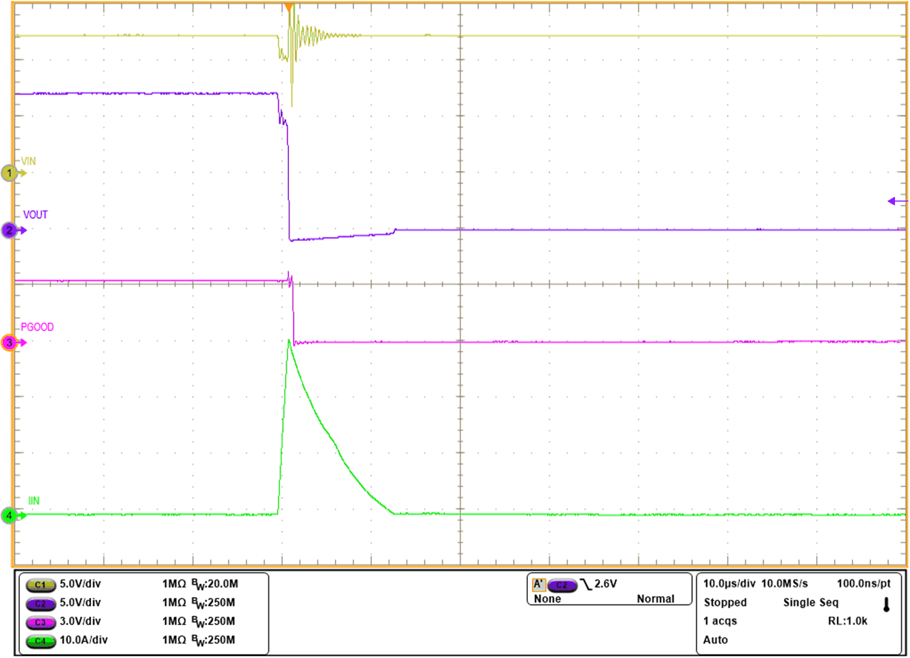
RILIM = 182 Ω
Figure 7-32 Output Hard Short-Circuit While ON (Zoomed In)
GUID-9D24A13B-30AE-4C09-AAAA-379702D882F9-low.png
RILIM = 511 Ω
Figure 7-34 Supply Line Transient Immunity - Adjacent Load Hot Unplug
GUID-74A7AA85-3885-4229-A2B3-49BB05BB715C-low.png
COUT = 220 μF CdVdt = 10 nF ROUT = Open
Figure 7-25 Startup With EN - dVdt Limited
GUID-E251C1CD-5D49-40D1-AD39-B456DDB79ECC-low.png
TPS259804x (16.7-V OVP variant)
Figure 7-27 Overvoltage Protection
GUID-20200807-CA0I-8JMR-H3J9-8LJ5PG6ZGKZR-low.gif
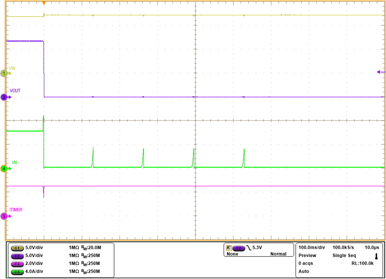
RILIM = 182 Ω CITIMER = 4.7 nF CRETRY_DLY = 2.2 nF, CNRETRY = 2.2 nF
Figure 7-29 Circuit Breaker - Auto-Retry
GUID-20200807-CA0I-H1K1-BNHT-J6NWBKGLT3HK-low.gif
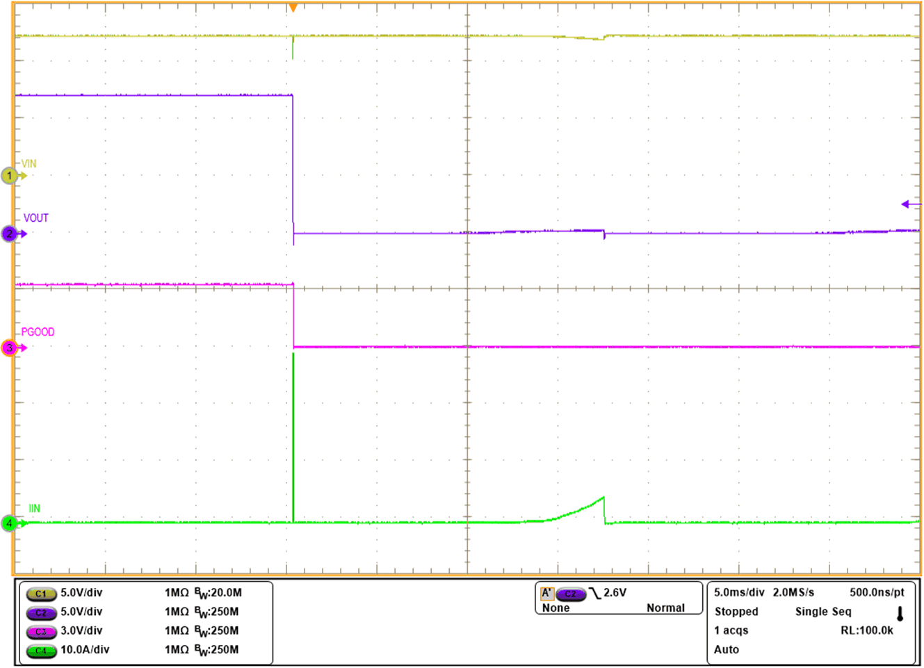
RILIM = 182 Ω
Figure 7-31 Output Hard Short-Circuit While ON
GUID-59682AFD-1DE8-4E9B-90C7-6C1834B96F43-low.png
RILIM = 332 Ω
Figure 7-33 Supply Line Transient Immunity - Input Voltage Step