JAJU819B April   2021  – June 2021


  1.   概要
  2.   リソース
  3.   特長
  4.   アプリケーション
  5.   5
  6. 1General Texas Instruments High Voltage Evaluation (TI HV EVM) User Safety Guidelines
  7. 2System Description
    1. 2.1 Key System Specifications
  8. 3System Overview
    1. 3.1 Block Diagram
    2. 3.2 Design Considerations
      1. 3.2.1 Basic Operation
      2. 3.2.2 PCMC PSFB using C2000
    3. 3.3 System Design Theory
      1. 3.3.1 Peak Current Mode Control (PCMC) Implementation
      2. 3.3.2 Zero Voltage Switching (ZVS) or Low Voltage Switching (LVS)
      3. 3.3.3 Synchronous Rectification
      4. 3.3.4 Slope Compensation
    4. 3.4 Highlighted Products
      1. 3.4.1 C2000™ MCU F28004x
  9. 4Hardware, Software, Testing Requirements, and Test Results
    1. 4.1 Required Hardware and Software
      1. 4.1.1 Hardware
      2. 4.1.2 Software
        1. 4.1.2.1 Software Control Flow
        2. 4.1.2.2 Incremental Builds
        3. 4.1.2.3 Procedure for running the incremental builds - PCMC
          1. 4.1.2.3.1 Build 1: Peak Current Loop Check with Open Voltage Loop
            1. 4.1.2.3.1.1 Objective
            2. 4.1.2.3.1.2 Overview
            3. 4.1.2.3.1.3 Procedure
              1. 4.1.2.3.1.3.1 Start CCS and Open a Project
              2. 4.1.2.3.1.3.2 Build and Load the Project
              3. 4.1.2.3.1.3.3 Debug Environment Windows
              4. 4.1.2.3.1.3.4 Using Real-Time Emulation
              5. 4.1.2.3.1.3.5 Run the Code
          2. 4.1.2.3.2 Build 2: Closed current and voltage loop (Full PSFB)
            1. 4.1.2.3.2.1 Objective
            2. 4.1.2.3.2.2 Overview
            3. 4.1.2.3.2.3 Procedure
              1. 4.1.2.3.2.3.1 Build and Load Project
              2. 4.1.2.3.2.3.2 Debug Environment Windows
              3. 4.1.2.3.2.3.3 Run the Code
      3. 4.1.3 Test results
  10. 5Design and Documentation Support
    1. 5.1 Design Files
      1. 5.1.1 Schematics
      2. 5.1.2 BOM
    2. 5.2 Software
    3. 5.3 Documentation Support
  11. 6Terminology
  12. 7About the Author
  13. 8Revision History

Synchronous Rectification

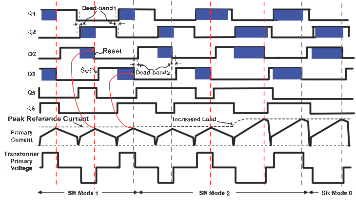
GUID-15EC973E-3BB6-4E7F-8B2B-C3703D6EE3CE-low.gif Figure 3-5 Synchronous Rectification mode

Synchronous rectifiers can work in one of the following three modes at any given time:

  1. Mode 0: This is the classical diode current doubler mode achieved by keeping synchronous rectifiers turned OFF. It is useful for very low load operations where synchronous rectifier switching losses are greater than the power savings obtained by synchronous rectification.
  2. Mode 1: In this mode the synchronous rectifier switches behave like ideal diodes. This mode is useful when operating at very low to low loads, typically when burst mode is being used. In this mode, synchronous rectifier MOSFETs are ON only when the corresponding diagonal bridge drive signals overlap.
  3. Mode 2: Useful for all other load conditions. In this mode, synchronous rectifier MOSFETs are OFF only when the corresponding opposite diagonal bridge drive signals overlap.

Figure 3-5 depict waveforms generated for driving the synchronous rectifier switches in these modes. It is important to implement mode transitions seamlessly without any glitches or anomalies on the PWM outputs even during large load transients or sudden phase shift change commands to ensure safe operation of the system.