SBAA572A February 2023 – May 2024 ADS9218 , ADS9219 , ADS9227
1
Introduction
Closed-loop systems, such as power-supplies, employ a feedback loop with control logic. The control algorithm can be implemented using either analog or digital circuits. Analog control loops optimize the control feedback for a specific load due to the fixed circuit hardware. In contrast, digital control loops can be optimized for a variety of loads. Furthermore, digital control loops offer higher accuracy because digital control loops are less prone to tolerances in passive components. This article discusses a low-latency control circuit using an analog-to-digital converter (ADC) and digital-to-analog converter (DAC) to implement a digital control loop. Feedback circuits optimized for current and voltage measurement respectively are discussed.
Digital Control Loop
A digital control loop uses an analog-to-digital converter (ADC) for sensing, a processor or FPGA for control and a digital-to-analog converter (DAC) to regulate the output of lab instruments such as power supplies, source measure units, and electronic loads. The main goal of a digital control loop in an instrument is to maintain a stable output voltage or current despite changes in the load conditions or input voltage. The control algorithm can be tuned according to the load to minimize settling time at the output of the instrument.
A typical digital control loop in an instrument includes the following components as shown in Figure 1:
- Measurement unit: This component measures the output voltage, current, or both, of the instrument and converts the measurement into a digital signal that can be processed by the controller.
- Controller: The controller receives the digital measurement of the output of the instrument and calculates an error signal, which is the difference between the measured output and the reference signal. The error signal is then processed by the control algorithm to determine the control inputs that need to be applied to the instrument.
- Control algorithm: This component processes the error signal to determine the control inputs that are applied to the instrument. The control algorithm can be based on a simple proportional-integral-derivative (PID) controller, or a more complex control algorithm such as a linear or nonlinear controller.
- Digital-to-analog converter (DAC): The DAC is responsible for converting the digital control signals into analog signals that can be applied to the instrument.

Figure 1 Digital Control Loop Block Diagram
The settling time or response time of the digital control loop depends on the speed at which the control algorithm can adjust the DAC input, to compensate for changes in the output voltage. The total delay in adjusting the DAC output voltage includes the following components:
- Time required for measuring the output signal in the measurement unit
- Time required for the control algorithm to generate a new setting for the DAC
- Time required for the DAC output to settle to required accuracy
To minimize the delay between the input signal and the response of the control loop, a low-latency signal chain to measure current and voltage are needed in the measurement path. The key specifications of the measurement unit signal chains are:
- DC Accuracy: An accurate measurement unit improves system accuracy because the measurement signal is used to adjust the DAC output signal.
- Wide Analog Bandwidth: This allows the system to quickly respond to transients in the input signal and changes in the load.
Current Feedback Signal Chain
As shown in Figure 2, the current feedback path consists of a precision shunt resistor, a current sense or instrumentation amplifier, and a low-latency precision analog-to-digital converter.

Figure 2 Current Feedback Circuit
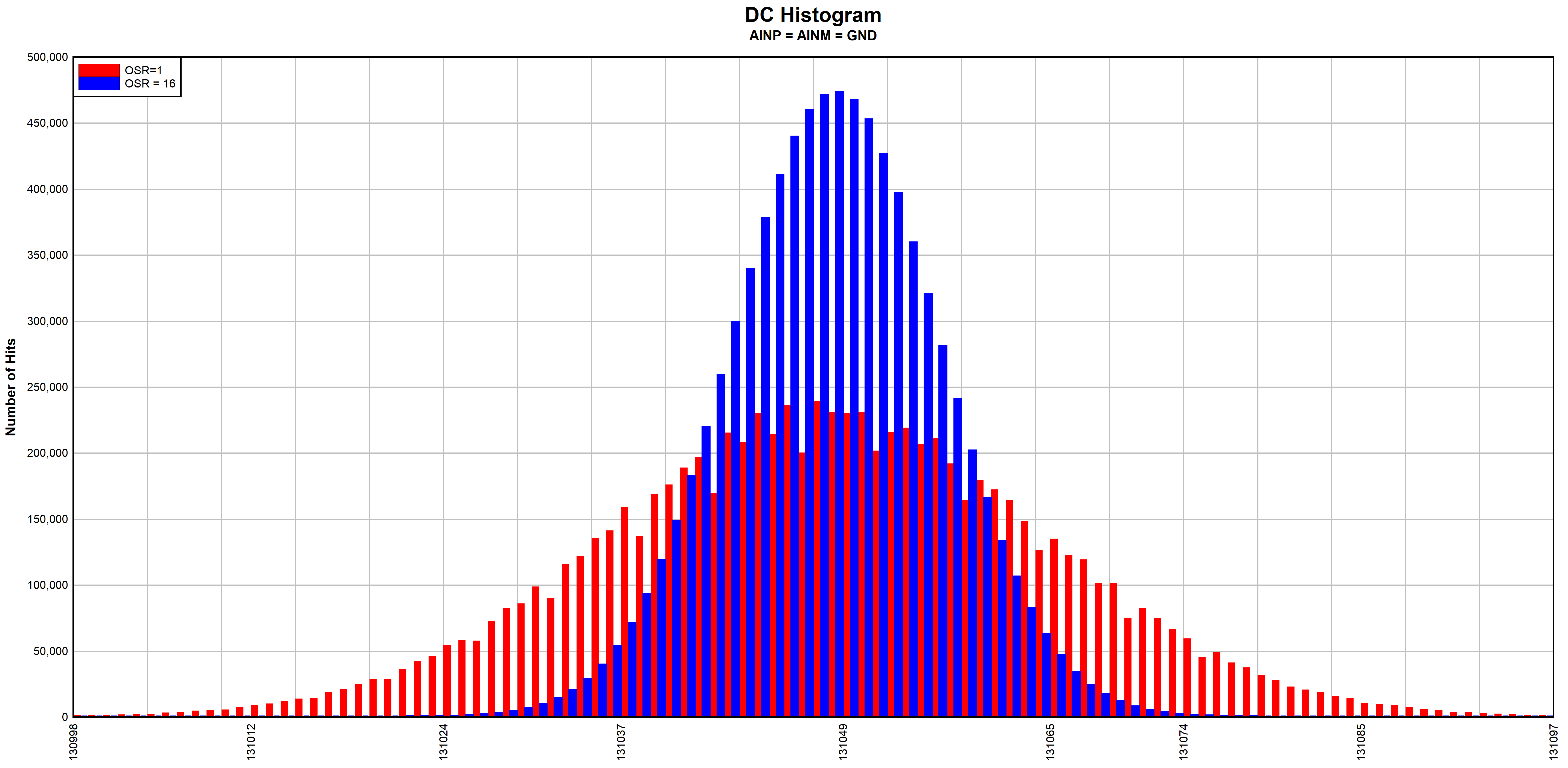
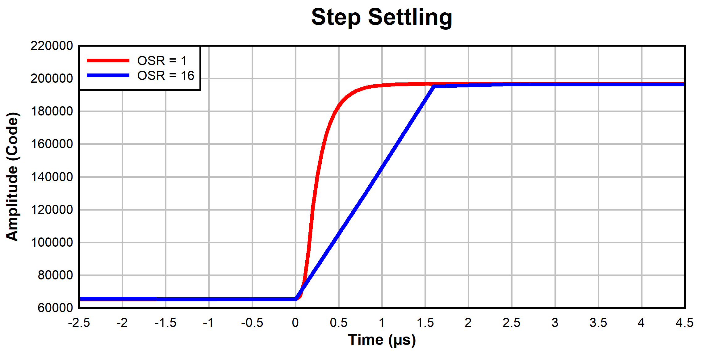
The example circuit uses the INA851 and ADS9219. The INA851 is a low-noise, high-speed, instrumentation amplifier with a fully differential output. The DC histogram and step settling plots with oversampling ratios (OSR) of 1 and 16 for this circuit are shown in Figure 3 and Figure 4 respectively.
 Figure 3 Current Feedback Circuit
DC Histogram
 Figure 4 Current Feedback Circuit
Step Settling with OSR = 1 and OSR = 16
Figure 4 Current Feedback Circuit
Step Settling with OSR = 1 and OSR = 16| OSR SETTING | STANDARD DEVIATION | SIGNAL-TO-NOISE RATIO |
|---|---|---|
| OSR = 1 | 14.87LSB | 75.89dB |
| OSR = 16 | 7.07LSB | 82.35dB |
Voltage Feedback Signal Chain
As shown in Figure 5, the voltage feedback path consists of a programmable gain amplifier (PGA), and a low-latency precision ADC.

Figure 5 Voltage Feedback Circuit
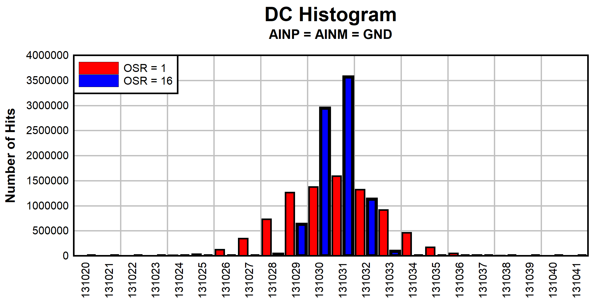
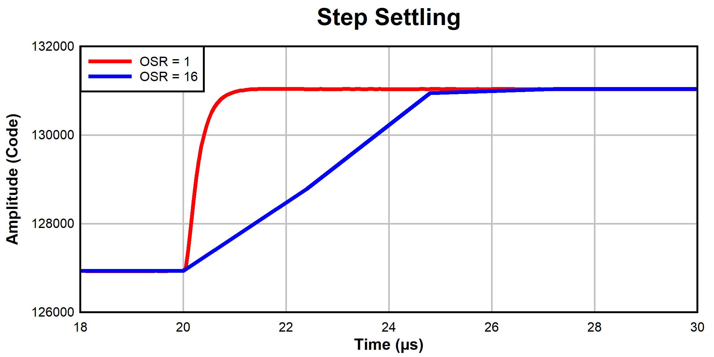
The example circuit uses PGA855 and ADS9219. The PGA855 is a low-noise, wide-bandwidth, programmable-gain instrumentation amplifier with a fully-differential output. The DC histogram and step settling plots for this circuit are shown in Figure 6 and Figure 7 respectively.

Figure 6 Voltage Feedback Circuit DC Histogram

Figure 7 Voltage Feedback Circuit Step Settling
| OSR SETTING | STANDARD DEVIATION | SIGNAL-TO-NOISE RATIO |
|---|---|---|
| OSR = 1 | 2.08LSB | 92.98dB |
| OSR = 16 | 0.86LSB | 100.6dB |
Precision, High-Speed Analog-to-Digital Converter
In the two circuits shown in Figure 2 and Figure 5, ADS9219 is used to accurately and quickly measure the system output signal. By converting the measured analog signal to a digital value at a high speed, the ADC helps to minimize the delay between the input signal and the response of the controller. The low-latency ADC improves the performance of the control loop by allowing the system to respond quickly and accurately to changes in the input signal
The ADS9219 is an 18-bit 20MSPS ADC based on successive approximation register (SAR) architecture that converts an analog signal to a digital value in 50ns. The controller must read the digital value from the ADC and this communication adds an additional time of 50ns. As a result, the controller can get a digital value from the measurement unit based on ADS9219 in a total time of 100ns.
The accuracy of the ADC affects the accuracy of the output of the instrument. The measurement accuracy depends on the thermal drift of errors in the measurement unit and the operating temperature range. The offset and gain errors in the measurement can be calibrated using a calibration circuit after the instrument powers-up to increase accuracy. The 18-bit resolution of ADS9219 enables high-accuracy measurements as shown in Table 3.
| CONDITION | INL (ppm) | OFFSET ERROR (ppm) | GAIN ERROR (ppm) | TUE (ppm) | ACCURACY |
|---|---|---|---|---|---|
| 25°C | 3.8 | 76.3 | 100 | 125.8 | 0.0125% |
| 25°C after calibration | 3.8 | 0 | 0 | 3.8 | 0.0003% |
| 25°C ±5°C after calibration | 3.8 | 5 | 10 | 11.81 | 0.0011% |
| 25°C ±25°C after calibration | 3.8 | 25 | 50 | 56.03 | 0.0056% |
Conclusion
Digital control loops are optimized for a variety of different loads and enable higher accuracy systems compared to analog control loops. To enable digital control loops, high accuracy, wide bandwidth signal-chains are needed in the measurement path. INA851 and PGA855 are fully-differential instrumentation amplifiers that can be paired with ADS9219 to implement wide bandwidth, high precision signal-chains in digital control loops.