SBAU394A April 2022 – September 2022
- ADS1285 Evaluation Module
- Trademarks
- 1 EVM Overview
- 2 ADS1285EVM-PDK Quick-Start Guide
- 3 EVM Analog Interface
- 4 Digital Interface
- 5 Power Supplies
- 6 Digital-to-Analog Converter
- 7 ADS1285EVM-PDK Initial Setup
- 8 ADS1285EVM-PDK Software Reference
- 9 ADS1285EVM-PDK Bill of Materials, PCB Layout, and Schematics
- 10References
- 11Revision History
8.6 DAC Configuration Tool
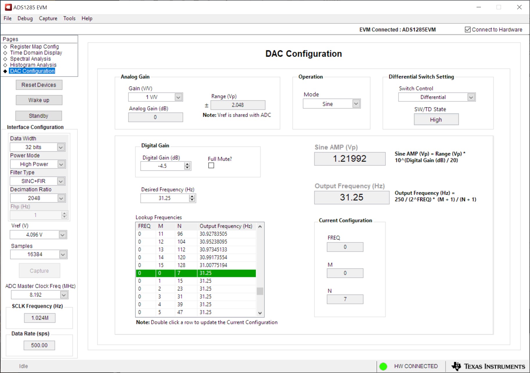
The DAC configuration tool page (Figure 8-6) controls the onboard DAC1282, a test DAC specifically designed to work with the ADS128x family of devices. As previously discussed in Section 6, the DAC output frequency is programmable from 0.5 Hz to 250 Hz and the magnitude is scaled by both analog and digital control. The analog gain is adjustable in 6-dB steps and the digital gain in 0.5-dB steps. The analog gain settings match those of the ADS1282 for testing at all gains with high resolution. More information about each setting can be found in the DAC1282 data sheet.
In general, the most important outcomes of changing the DAC are to understand the mode, output amplitude, and output frequency (if applicable). In the middle, the Operation box shows the Mode drop-down, which can be: Sine, DC, digital pulse, and pulse.
For Sine, the amplitude is determined by a combination of the analog gain and digital gain settings. In addition, the DAC page uses the Vref (V) drop-down menu to calculate the values in the gray boxes, although the DAC does not need to know the reference voltage to function. As a result, review the Sine AMP (Vp) calculation, in combination with the ADC gain on the register map page, to understand the output code and voltage of the ADC. The frequency is determined by typing a desired frequency into the Desired Frequency (Hz) text box. The GUI automatically displays the closest Freq, M, and N values to achieve the desired output frequency that are eventually written into the DAC registers. These options dynamically change when selecting DC, digital pulse, or pulse.
As mentioned in Section 3.1, the direct DAC output or the DAC integrated switches can be used. Assuming the correct hardware is changed to support the integrated switches, the state of the switches can be changed using the Switch Control drop-down.
The settings in Figure 8-6, in combination with selecting 2 V/V for PGA_GAIN and Input 2 for MUX, create the time domain and spectral analysis plots in Figure 8-3 and Figure 8-4, respectively.
 Figure 8-6 DAC Configuration Tool
Page