SBOA442 March 2021 TMP107 , TMP107-Q1
4 TMP107-Q1 Over the RS-485 Bus
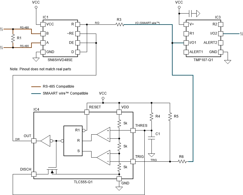
Figure 4-1 shows the implementation with the RS-485 transceiver. The transceiver features complementary enable signals for the transmitter and the receiver. This integrated functionality replaces the SN74LVC2G241 buffer from the CAN-based circuit. For this reason, the DIR signal from the TLC555-Q1 timer connects directly to the DE and ~RE signals.
 Figure 4-1 Simplified Circuit Diagram
for Interfacing the TMP107-Q1 Over the RS-485 bus
Figure 4-1 Simplified Circuit Diagram
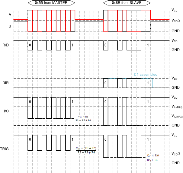
for Interfacing the TMP107-Q1 Over the RS-485 busFigure 4-2 represents ideal waveforms for the circuit with the RS-485 transceiver.
 Figure 4-2 Ideal Waveforms for the
RS-485 to SMAART wire™
Interface Converter Circuit
Figure 4-2 Ideal Waveforms for the
RS-485 to SMAART wire™
Interface Converter Circuit(Example Only)