SBOA518 January 2022 TMCS1100 , TMCS1100-Q1 , TMCS1101 , TMCS1101-Q1 , TMCS1107 , TMCS1107-Q1 , TMCS1108 , TMCS1108-Q1
3 Grounding
A key feature of the TMCS110x device family is temperature compensation. This allows a given TMCS110x device to achieve a low-sensitivity drift of ±0.5% over temperature and lifetime. This compensation is achieved through internal circuitry that utilizes a clock, which contains pulsing components, and therefore requires a properly-designed ground path. While a low-resistance path between device ground and the central system ground is a good practice in general, the digital clock provides a dynamic current component that can further influence measurement precision. Therefore, Equation 2 is used to approximate what kind of offset might be observed for a given device ground to system ground return path, where the values of resistance and inductance are quantifiable from the planes or traces between the GND pin of the TMCS1100 and the system ground.
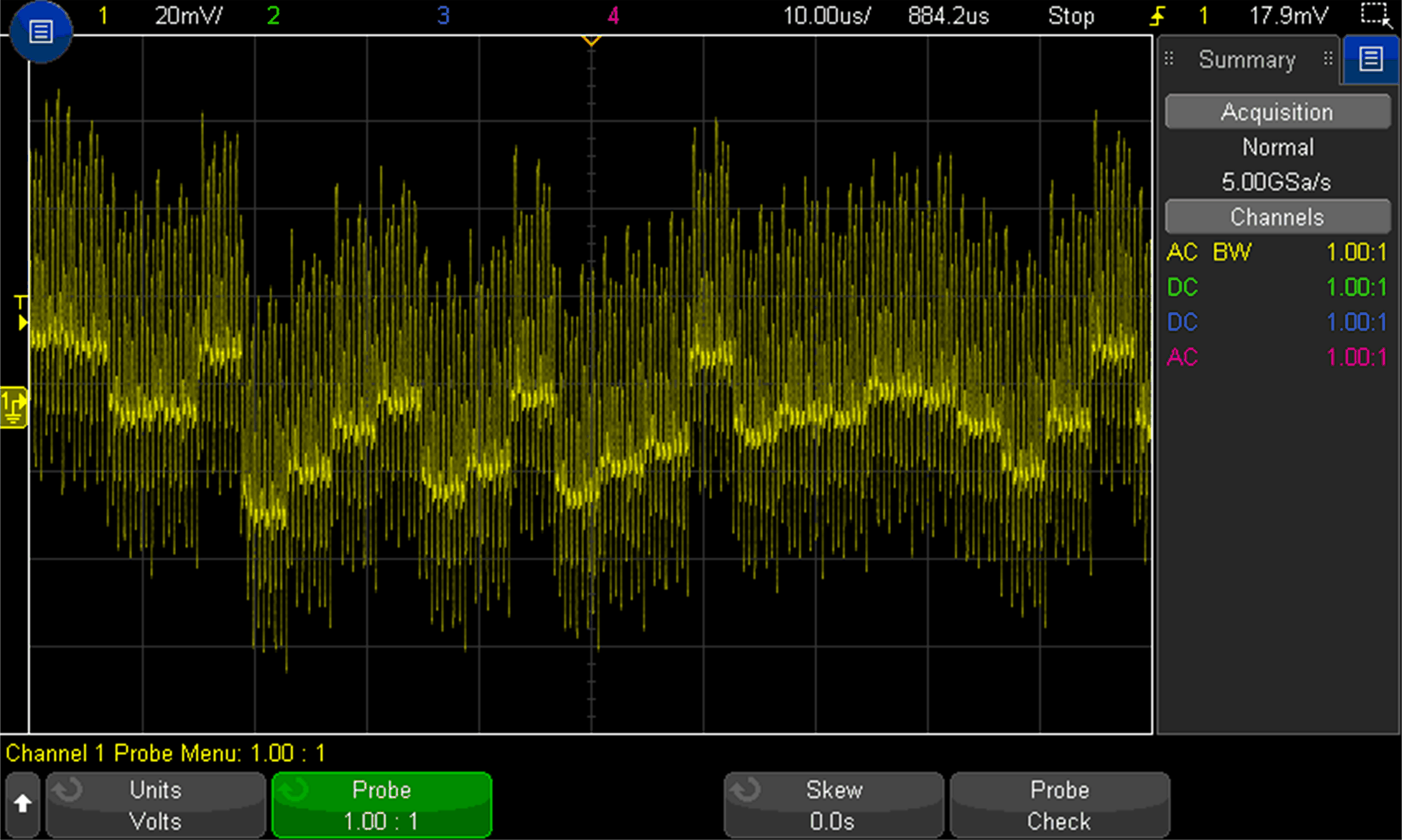
As the path to system ground becomes more complex, the effect of these artifacts becomes more apparent as added offset and noise on the output of the device. To demonstrate this, a long, discrete coiled wire was used in place of the ground plane on a TMCS1100EVM to emulate a long trace between the GND pin and system GND of the module. In addition, the bypass capacitor was also removed from the EVM to provide a worst-case look at the effects of these artifacts on the device. TMCS1100EVM With "Poor" Inductive Ground Path shows the output of the A2 device variant in this state, with no input current supplied to the device.
 Figure 3-1 TMCS1100EVM With "Poor" Inductive
Ground Path
Figure 3-1 TMCS1100EVM With "Poor" Inductive
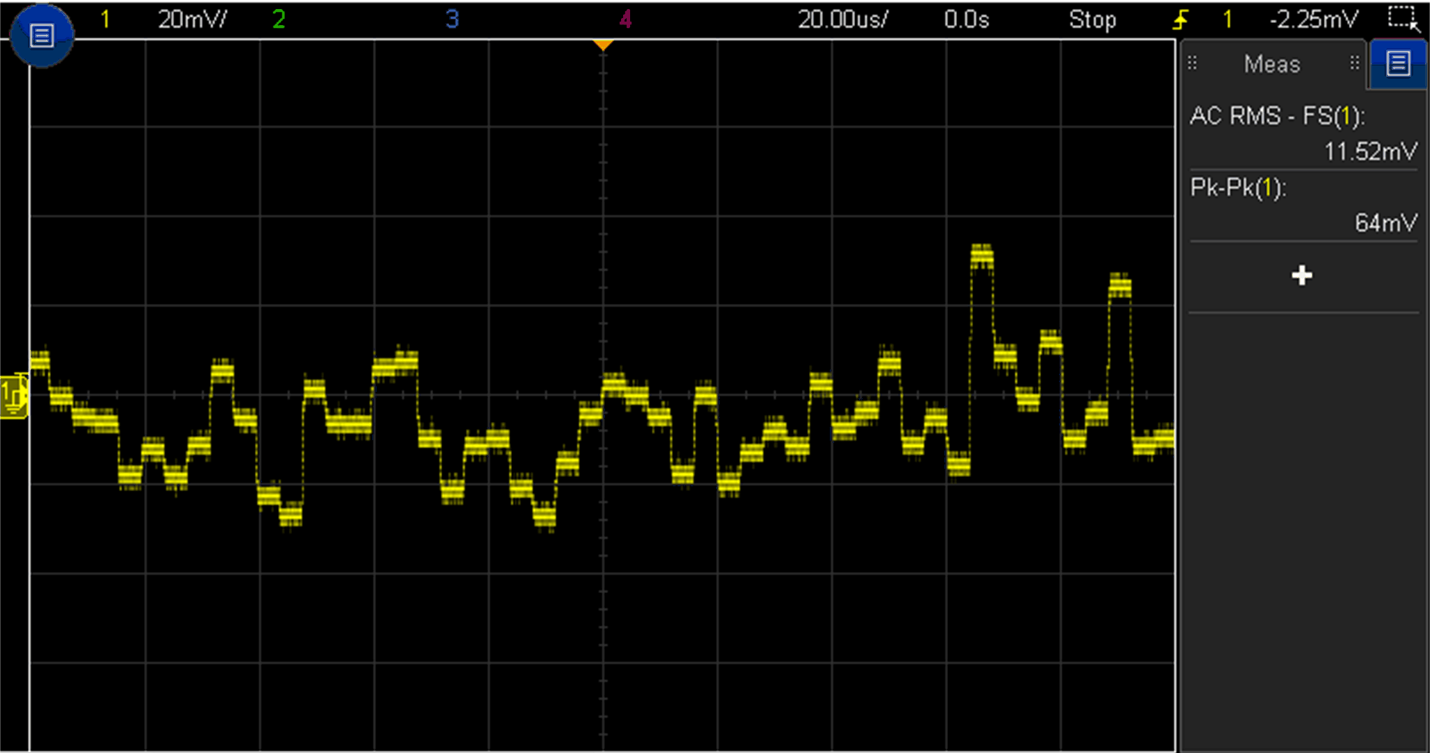
Ground PathAn ideal grounding path is a direct path from the GND pin of the device to the system GND of the board, using as wide of a trace as possible to minimize resistance and inductance between the connection points. A GND plane as used on the TMCS1100EVM is ideal. TMCS1100EVM Default "Good" Ground Path shows the output of the A1 variant under ideal grounding conditions.
 Figure 3-2 TMCS1100EVM Default "Good" Ground
Path
Figure 3-2 TMCS1100EVM Default "Good" Ground
PathNote that the "good" ground of the device still retains bouncing artifacts. This is expected as systematic noise comes from the sampling integrator used to compensate for temperature and lifetime drift, and is discussed in depth in the next section. In most designs, a wide ground plane as mentioned is not always achievable, but consideration must be given to how the device GND pin interfaces with the true ground of the system for best performance.