SBOU256 December 2020 BUF634A
6 Layout
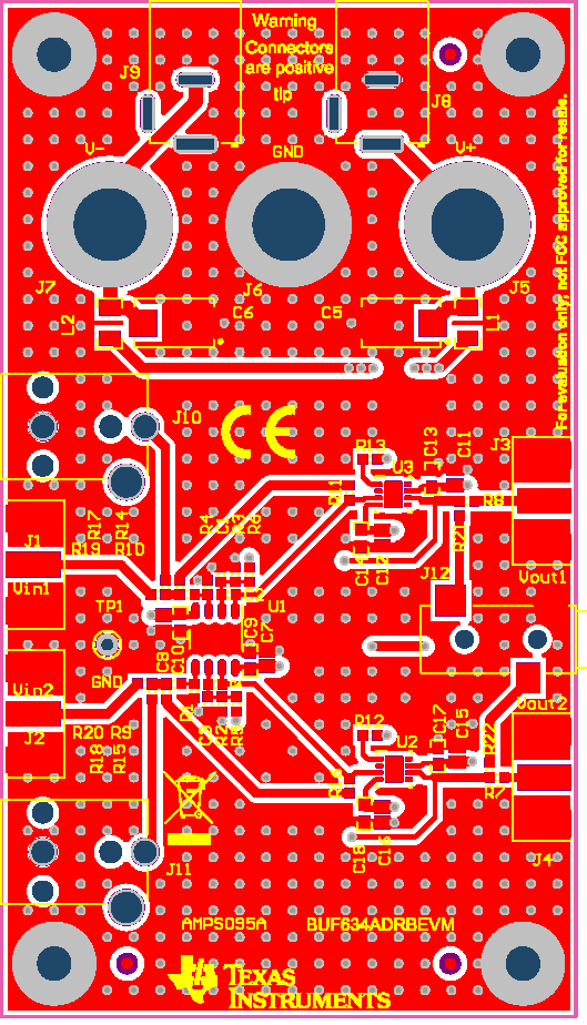
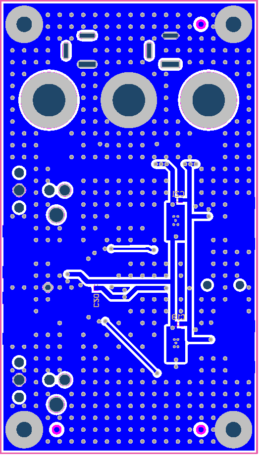
Figure 6-1 and Figure 6-2 illustrate the layers for the BUF634ADRBEVM.
 Figure 6-1 BUF634ADRBEVM Top Layer
 Figure 6-2 BUF634ADDAEVM Bottom Layer
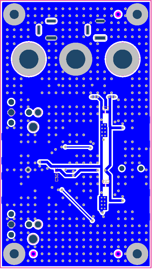
Figure 6-3 through Figure 6-4 illustrate the various layout silk screens for the BUF634ADDAEVM.
 Figure 6-3 BUF634ADRBEVM Top Layer
 Figure 6-4 BUF634ADDAEVM Bottom Solder