SBOU301A July 2023 – January 2024 LOG200
3.2 PCB Layout
The LOG200EVM is a four-layer PCB design. Figure 4-3 to Figure 4-7 show the PCB layer illustrations.
The top layer routes the sensitive input current signal path traces. The logarithmic amplifier is optimized to perform current measurements across several decades. At the low current level ranges, leakage current can cause significant errors. To minimize leakage current paths, a complete guard ring is implemented with traces that encircle the complete signal path of each high-impedance current input of the log amplifier. The guard presents a low-impedance path for leakage currents of equal potential to the high-impedance traces that are being guarded. The guard traces are driven to the input common-mode voltage (VCM); therefore, the current flowing between the input current traces and the guard is negligible because both traces are similarly at the same potential.
The LOG200EVM provides a footprint to connect a photodiode to the I1 input pin. The photosensor is kept in close proximity to the I1 input to minimize parasitic capacitance. The evaluation board provides all the necessary photosensor and adaptive bias circuit connections through resistor R2, R3 and optional capacitors C1, C3. For a detailed explanation, refer to the photodiode connections section of the User Guide.
Decoupling capacitors C7, C8 and C11 are positioned on the top layer as close as possible to the power-supply pins of the device. Similarly, reference bypass capacitor C12 and C14 are located in close proximity to the reference pins.
The second internal layer is a dedicated to the power supplies connections and contains a common-mode (VCM) plane. The third internal layer and bottom layers contain a ground plane and route additional auxiliary amplifier/reference signals.
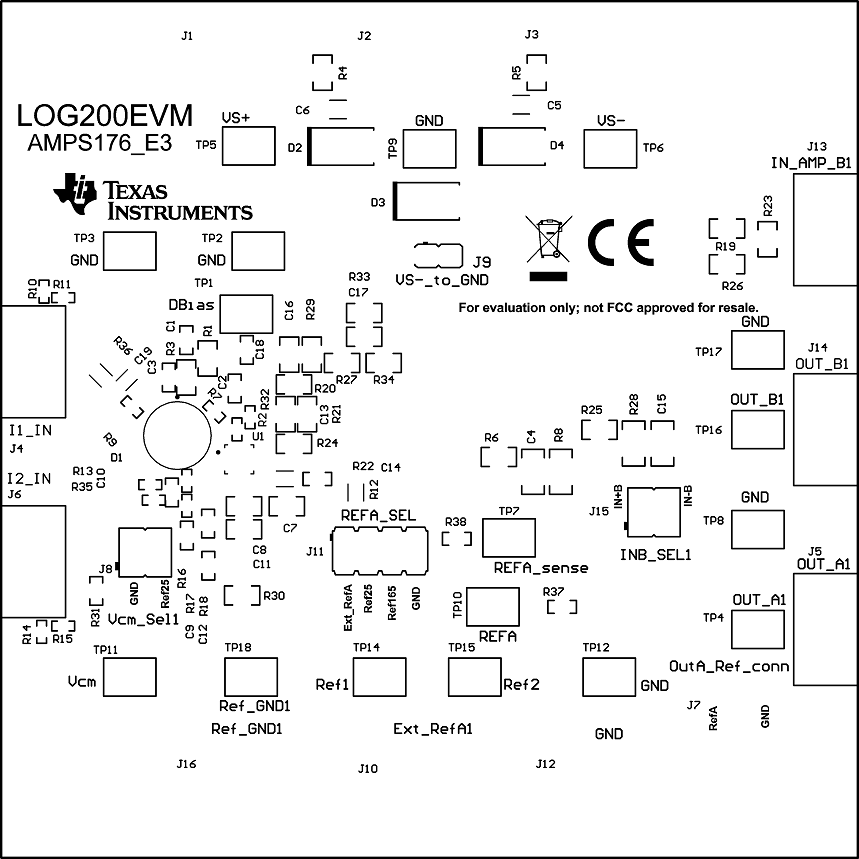 Figure 3-3 Top Overlay PCB Layout
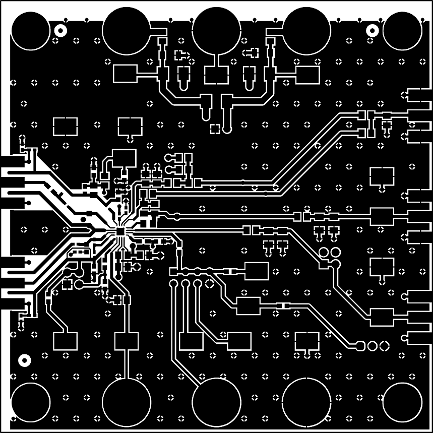 Figure 3-4 Top Layer PCB Layout
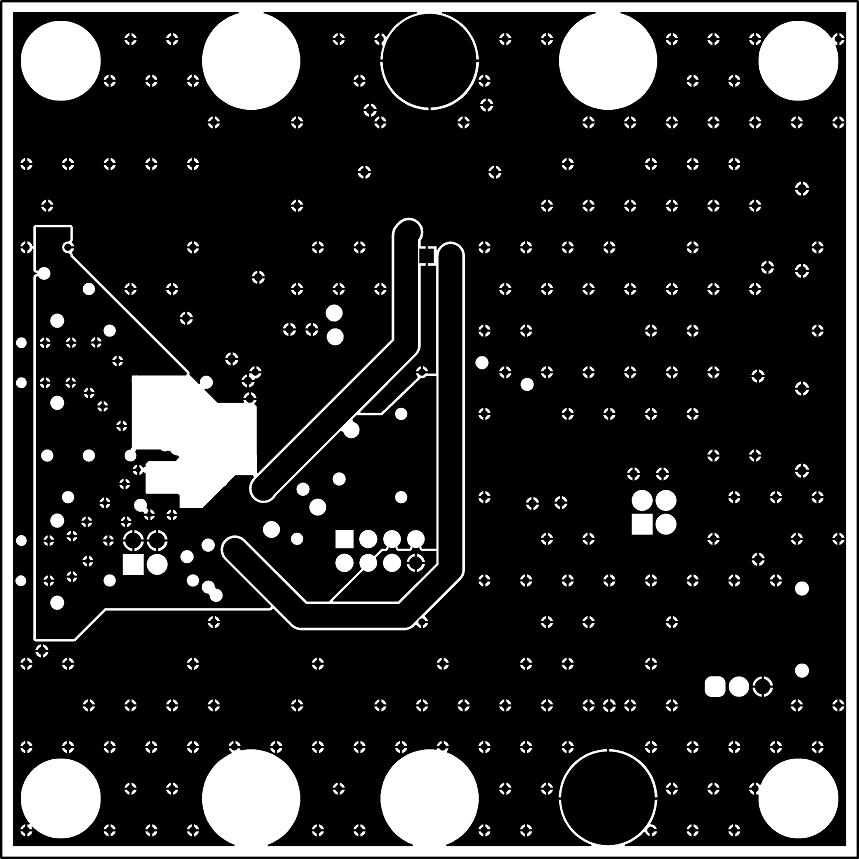 Figure 3-5 Mid Layer 1 PCB Layout
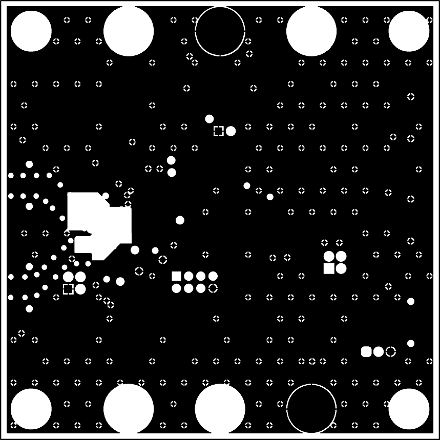 Figure 3-6 Mid Layer 2 PCB Layout
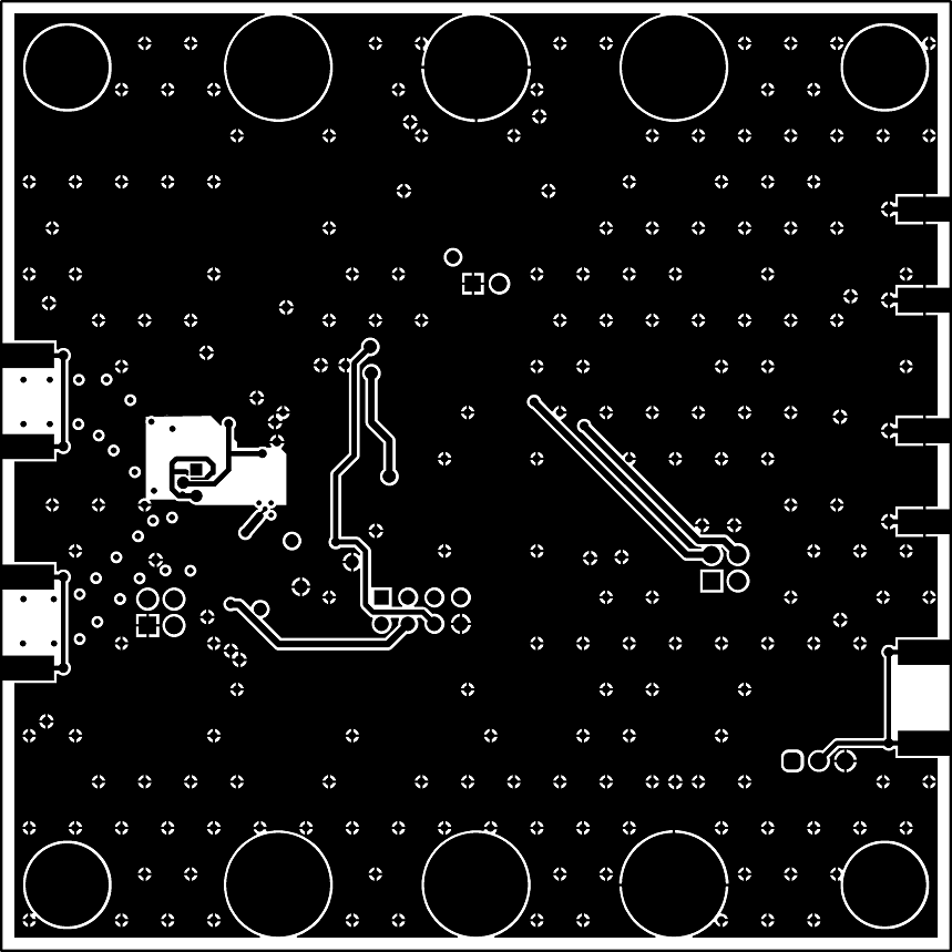 Figure 3-7 Bottom Layer PCB Layout