SCDU025 May 2021 TMUX646
6 PCB Layouts
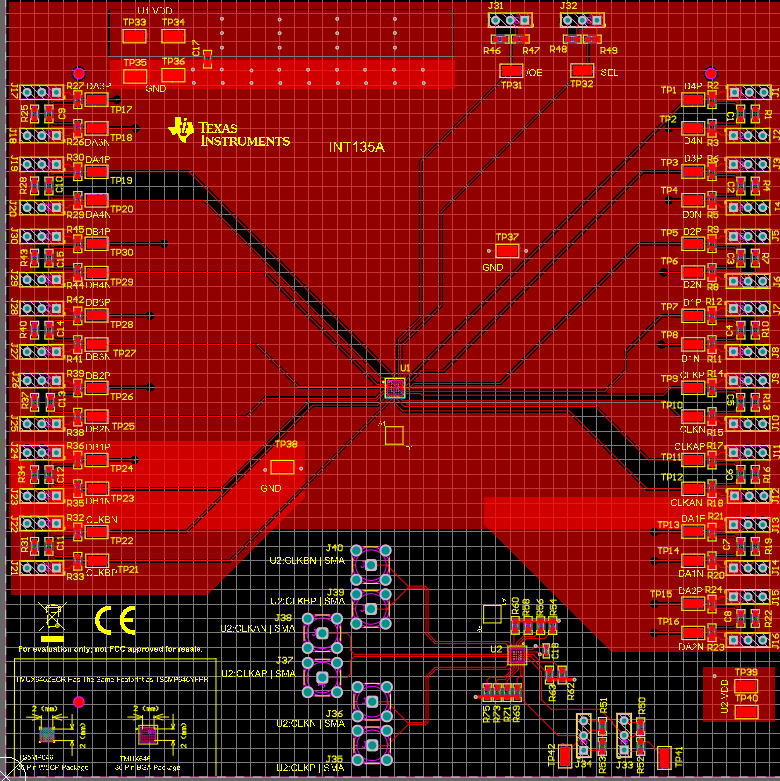
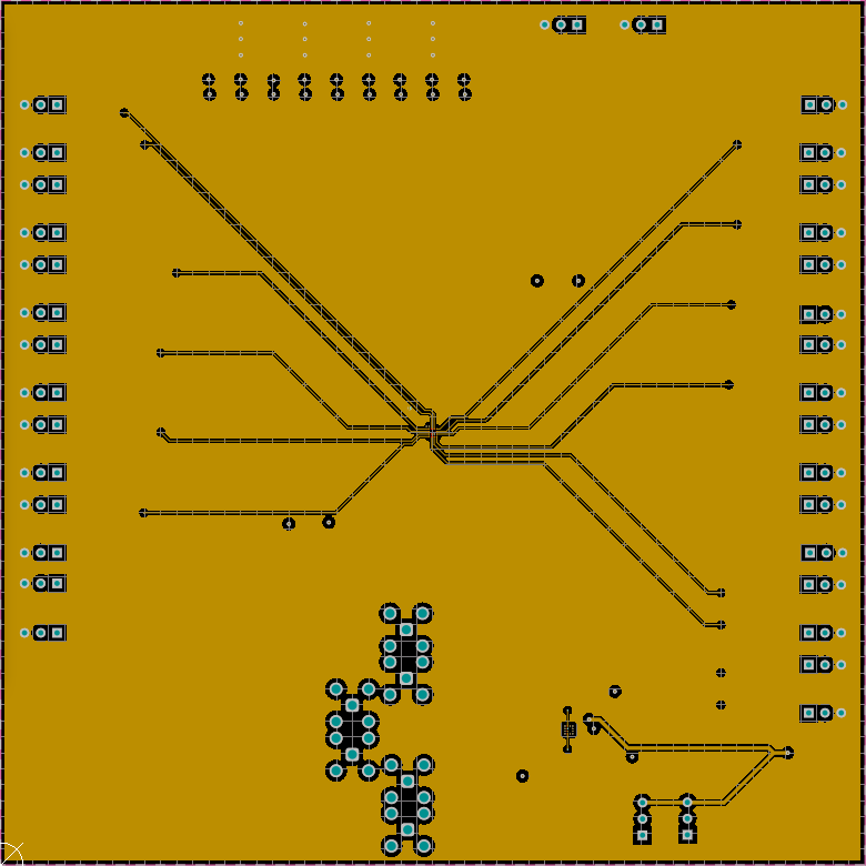
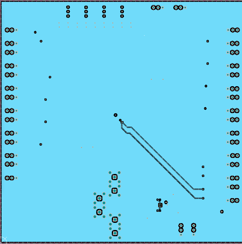
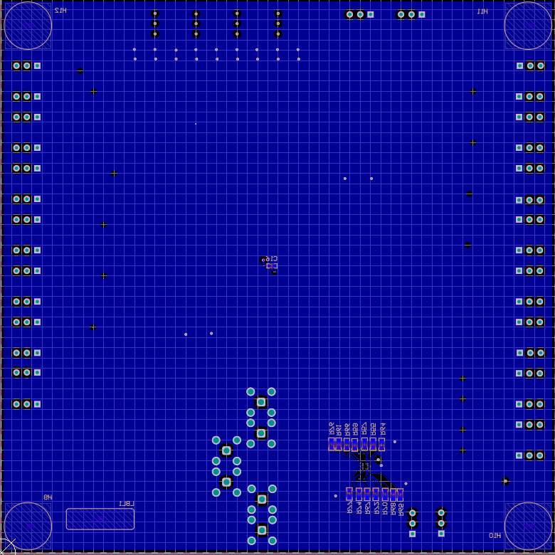
Below are the layouts for the TMUX646EVM.
 Figure 6-1 Top View Illustration of the TMUX646EVM Layout
 Figure 6-2 First Internal Layer Illustration of the TMUX646EVM Layout
 Figure 6-3 Second Internal Layer Illustration of the TMUX646EVM Layout
 Figure 6-4 Bottom Layer Illustration of the TMUX646EVM Layout