SCEA117 July 2022 SN74HCS164 , SN74HCS164-Q1 , SN74HCS165 , SN74HCS165-Q1 , SN74HCS595 , SN74HCS595-Q1
2.2 Operating over Large Distances
When designing with small circuits, the time it takes electric signals to travel is typically negligible. As circuits get physically larger, delays increase and can become problematic. For example, in large digital billboard signs, the distance from the controller to the farthest corner of the display could be fifty feet or more. This large distance can cause problems for designing with shift registers.
In the ideal case (light speed in a vacuum), signals could propagate across 1 ft in approximately 1 ns, however we find in practice that signals in a transmission line (or on a PCB) tend to propagate at about half that speed, so 2 ns is a more realistic estimate. Additionally, this does not take into account the physical position on the line and other transmission line effects.
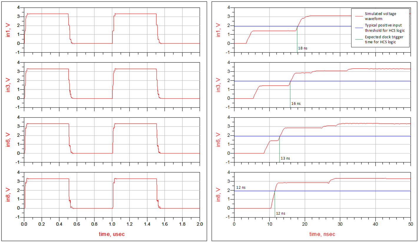
 Figure 2-2 (left) Simulated Clock
Waveforms Received by the First, Third, Sixth, and Eighth Shift Registers.
(right) Zoomed Versions of the Same Four Waveforms to More Clearly Show the
Rising Edge.
Figure 2-2 (left) Simulated Clock
Waveforms Received by the First, Third, Sixth, and Eighth Shift Registers.
(right) Zoomed Versions of the Same Four Waveforms to More Clearly Show the
Rising Edge.Utilizing the available IBIS models on TI.com and the PathWave ADS simulator, Figure 2-2 shows the same clock signal arriving at eight different shift registers spaced six inches (1 ns delay) apart from each other. The right-hand side is zoomed in on the rising edge to provide more details. The “stair step” waveform shown is caused by the transmission line effects (reflections), an explanation of which are beyond the scope of this application report.
Looking at the clock trigger times marked it green, it can be seen that there is a 6 ns delay from when the last shift register is triggered to when the first one is triggered. This seems counter-intuitive, but looking closer at the waveform shows that the wave does reach in1 first at approximately 4 ns, however the reflections cause the waveform to seemingly pause at approximately half the total voltage from approximately 5 ns until 18 ns.
There are two major issues that need to be considered from the input signals shown in Figure 2-2. First, the mismatch in clock trigger timing can cause data loss when shift registers are daisy-chained together. In the example shown, only one buffer is used to drive the line in order to better show the transmission line effects, however it is common practice to redrive signals using buffers throughout a system, which can help with signal integrity, but will add additional delays. For an explanation of how this can cause data loss, see the explanation in Section 2.3.
Second, although in this case the “stair step” in the input signals is only 6 ns, it does illustrate that long transmission lines can create slow and possibly non-monotonic edges. For many standard CMOS devices, slow edges and holding an input voltage near VCC/2 can cause internal oscillations, excessive power consumption, and reduction in reliability. Schmitt-trigger architecture inputs will prevent all of these issues, so the HCS logic family is ideal to handle this type of operation.
For a full explanation on how slow inputs affect standard CMOS devices, see the application report Implications of Slow or Floating CMOS Inputs. For a full explanation on the benefits of the Schmitt-trigger architecture, see the application report Understanding Schmitt Triggers.