SFFS800 January 2024 LM74500-Q1
4 Pin Failure Mode Analysis (Pin FMA)
This section provides a Failure Mode Analysis (FMA) for the pins of the LM74500-Q1. The failure modes covered in this document include the typical pin-by-pin failure scenarios:
- Pin short-circuited to Ground (see Table 4-2)
- Pin open-circuited (see Table 4-3)
- Pin short-circuited to an adjacent pin (see Table 4-4 andTable 4-5)
- Pin short-circuited to supply (see Table 4-5)
Table 4-2 through Table 4-5 also indicate how these pin conditions can affect the device as per the failure effects classification in Table 4-1.
| Class | Failure Effects |
|---|---|
| A | Potential device damage that affects functionality |
| B | No device damage, but loss of functionality |
| C | No device damage, but performance degradation |
| D | No device damage, no impact to functionality or performance |
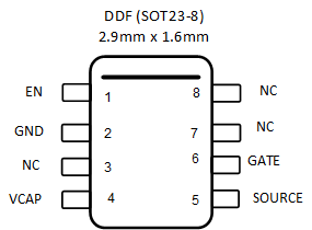
Figure 4-1 shows the LM74500-Q1 pin diagram. For a detailed description of the device pins please refer to the Pin Configuration and Functions section in the LM74500-Q1 data sheet.
 Figure 4-1 Pin Diagram (DDF
Package)
Figure 4-1 Pin Diagram (DDF
Package)The pin FMA is provided under the assumption that the device is operating under the specified ranges within the Recommended Operating Conditions section of the data sheet.
| Pin Name | Pin No. | Description of Potential Failure Effect(s) | Failure Effect Class |
|---|---|---|---|
| EN | 1 | Device will not power up as enable pin is shorted to ground. | B |
| GND | 2 | No effect on the performance. | D |
| N.C | 3,7,8 | No effect on the performance. | D |
| VCAP | 4 | Device can be damaged due to internal conduction. | A |
| SOURCE | 5 | This is equivalent to input supply short to GND. Device will not power up. | B |
| GATE | 6 | Device can get damaged due to internal conduction. | A |
| Pin Name | Pin No. | Description of Potential Failure Effect(s) | Failure Effect Class |
|---|---|---|---|
| EN | 1 | Device will be in shutdown mode due to internal pull down on EN pin. | B |
| GND | 2 | Device may not power up. | B |
| N.C | 3,7,8 | No effect on the performance. | D |
| VCAP | 4 | Charge pump voltage will not generate. Gate drive voltage will not be available. | B |
| SOURCE | 5 | Device will not power up. | B |
| GATE | 6 | Gate drive for external FET will not be available. External FET will be off. | B |
| Pin Name | Pin No. | Shorted to | Description of Potential Failure Effect(s) | Failure Effect Class |
|---|---|---|---|---|
| EN | 1 | GND | Device will be in shutdown mode. | B |
| GND | 2 | N.C | No effect on the device performance. | D |
| N.C | 3 | VCAP | No effect on the device performance. | D |
| VCAP | 4 | — | VCAP is a corner pin. No effect on the device performance. | D |
| SOURCE | 5 | GATE | External FET will not turn on as GATE pin is shorted to SOURCE. | B |
| GATE | 6 | N.C | No effect on the device performance. | D |
| N.C | 7 | N.C | No effect on the device performance. | D |
| N.C | 8 | — | Corner pin; no effect on the device performance. | D |
| Pin Name | Pin No. | Description of Potential Failure Effect(s) | Failure Effect Class |
|---|---|---|---|
| EN | 1 | Device will always be ON as enable pin is pulled high. Device shutdown feature will not be available. | B |
| GND | 2 | This condition is equivalent input supply shorted to ground. Device will not power up. | B |
| N.C | 3, 7, 8 | No effect on the device performance. | D |
| VCAP | 4 | Charge pump voltage will not build up and gate drive voltage will be disabled. | B |
| SOURCE | 5 | No effect on the device performance. | D |
| GATE | 6 | External FET will not turn on as gate drive voltage will not be applied to external FET GATE pin. | B |