SLAA502A July 2011 – September 2023 MSP430FR5720 , MSP430FR5721 , MSP430FR5722 , MSP430FR5723 , MSP430FR5724 , MSP430FR5725 , MSP430FR5726 , MSP430FR5727 , MSP430FR5728 , MSP430FR5729 , MSP430FR5730 , MSP430FR5731 , MSP430FR5732 , MSP430FR5733 , MSP430FR5734 , MSP430FR5735 , MSP430FR5736 , MSP430FR5737 , MSP430FR5738 , MSP430FR5739
2.2 Write Endurance
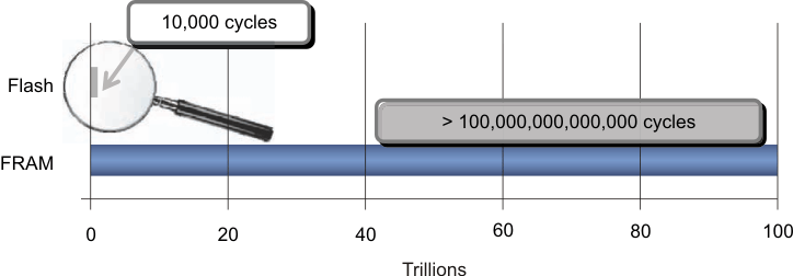
 Figure 2-3 Write Endurance
The FRAM technology provides write endurance that is superior to other non-volatile memory technologies as illustrated in Figure 2-3. For the data logger application, this translates into a much longer lifetime with less complexity; assuming the data logger has to store one set of data each second and it always uses the same addresses, this would translate into a lifetime of a data logger using Flash memory of less than three hours (assuming a Flash with 104 cycles divided by 1 cycle per second). The same data logger using FRAM would achieve a theoretical life time of more than 3 million years making use of the more than 1014 write cycles FRAM offers. To increase the life time of the Flash-based data logger, complex wear leveling algorithms together with additional Flash memory space would be required. The wear leveling algorithms would try to make use of multiple Flash cells and use them more or less equally. For FRAM, wear leveling is not required, which significantly reduces the complexity and also the amount of memory required.