SLAAE45 September 2021 TMUXHS4412
2.2 PCIe® High-Speed Signal Layout Guidelines
- For PCIe® high-speed signals, design trace impedance so as to minimize the reflections in traces. Control the trace impedance to be as close as possible to the recommended values in Table 2-1.
- Keep the total trace length for signal pairs to a minimum.
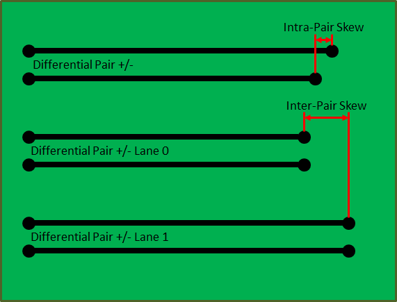
- Match the etch lengths of the relevant differential pair traces. Make sure intra-pair skew is within 5 mils for the PCIe® standard. There is no need to match inter-pair skew.
 Figure 2-1 Differential Pair Intra-Pair Skew and Inter-Pair Skew
 - To minimize crosstalk in high-speed interface implementations, the spacing between the signal pairs must be a minimum of 5 times the width of the trace.
- When possible, route high-speed differential pair signals on the top or bottom layer of the PCB with an adjacent GND layer. TI does not recommend stripline routing of the high-speed differential signals.
- Void right-angle bends in a trace and try to route them at least with two 45° corners. To minimize any impedance change, the best routing is a round bend (see Figure 2-2)
 Figure 2-2 Poor and Good Right Angle Bends