SLAAEG4 October   2023 MSPM0C1104 , MSPM0L1306


  1.   1
  2.   Abstract
  3.   Trademarks
  4. MSPM0C Hardware Design Check List
  5. Power Supplies in MSPM0C Devices
    1. 2.1 Digital Power Supply
    2. 2.2 Analog Power Supply
    3. 2.3 Built-in Power Supply and Voltage Reference
    4. 2.4 Recommended Decoupling Circuit for Power Supply
  6. Reset and Power Supply Supervisor
    1. 3.1 Digital Power Supply
    2. 3.2 Power Supply Supervisor
      1. 3.2.1 Power-On Reset (POR) Monitor
      2. 3.2.2 Brownout Reset (BOR) Monitor
      3. 3.2.3 POR and BOR Behavior During Supply Changes
  7. Clock System
    1. 4.1 Internal Oscillators
      1. 4.1.1 Internal Low-Frequency Oscillator (LFOSC)
      2. 4.1.2 Internal System Oscillator (SYSOSC)
    2. 4.2 External Clock Input (xFCLK_IN)
      1. 4.2.1 LFCLK_IN
      2. 4.2.2 HFCLK_IN
    3. 4.3 External Clock Output (CLK_OUT)
    4. 4.4 Frequency Clock Counter (FCC)
  8. Debugger
    1. 5.1 Debug Port Pins and Pinout
    2. 5.2 Debug Port Connection With Standard JTAG Connector
      1. 5.2.1 Standard XDS110
      2. 5.2.2 Lite XDS110 (MSPM0 LaunchPad™ kit)
  9. Key Analog Peripherals
    1. 6.1 ADC Design Considerations
  10. Key Digital Peripherals
    1. 7.1 Timer Resources and Design Considerations
    2. 7.2 UART and LIN Resources and Design Considerations
    3. 7.3 I2C and SPI Design Considerations
  11. GPIOs
    1. 8.1 GPIO Output Switching Speed and Load Capacitance
    2. 8.2 GPIO Current Sink and Source
    3. 8.3 Open-Drain GPIOs Enable 5-V Communication Without a Level Shifter
    4. 8.4 Communicate With 1.8-V Devices Without a Level Shifter
    5. 8.5 Unused Pins Connection
  12. Layout Guides
    1. 9.1 Power Supply Layout
    2. 9.2 Considerations for Ground Layout
      1. 9.2.1 What is Ground Noise?
    3. 9.3 Traces, Vias, and Other PCB Components
    4. 9.4 How to Select Board Layers and Recommended Stack-up
  13. 10References

Lite XDS110 (MSPM0 LaunchPad™ kit)

The MSPM0 LaunchPad kit include the XDS110 (Lite) circuit. You can also use this debugger to download your firmware into MSPM0 device. Figure 5-5 shows the LP-MSPM0C1104 circuit.

2.54-mm probe: This port supports the SWD protocol and includes a 5-V or 3.3-V power supply. You can connect SWDIO SWCLK 3V3 GND to the board and download firmware into the MSPM0C device.
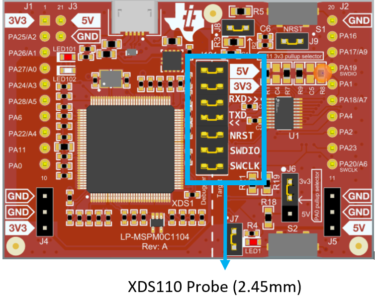
GUID-8CC95932-0099-4D07-B789-138C7FA256DF-low.png Figure 5-5 LP-MSPM0C1104
Note:
  • Standard XDS110 support level shift for debug ports, XDS110 just support 3.3v probe level.
  • TI does not recommend using the XDS110 to power other devices except the MSPM0C MCU. The XDS110 integrates an LDO with limited current drive capability.