SLLA470A April 2020 – October 2020 TLIN1028S-Q1
3 Pin Failure Mode Analysis (Pin FMA)
This section provides a Failure Mode Analysis (FMA) for the pins of the TLIN10283S-Q1 and TLIN10285S-Q1. The failure modes covered in this document include the typical pin-by-pin failure scenarios:
- Pin short-circuited to Ground (see Table 3-2)
- Pin open-circuited (see Table 3-3)
- Pin short-circuited to an adjacent pin (see Table 3-4)
- Pin short-circuited to VSUP (see Table 3-5)
- Pin short-circuited to VCC (see Table 3-6)
Table 3-2 through Table 3-6 also indicate how these pin conditions can affect the device as per the failure effects classification in Table 3-1.
| Class | Failure Effects |
|---|---|
| A | Potential device damage that affects functionality |
| B | No device damage, but loss of functionality |
| C | No device damage, but performance degradation |
| D | No device damage, no impact to functionality or performance |
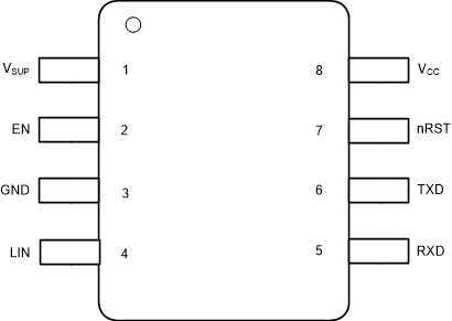
Figure 3-1 shows the TLIN10283S-Q1 and TLIN10285S-Q1 pin diagram. For a detailed description of the device pins please refer to the 'Pin Configuration and Functions' section in the TLIN10283S-Q1 and TLIN10285S-Q1 datasheet.
 Figure 3-1 Pin Diagram
Following are the assumptions of use and the device configuration assumed for the Pin FMA in this section:
- All conditions within recommended operating conditions.
-
VCC = 4.9 to 5.1 V for TLIN10285S-Q1
-
VCC = 3.23 to 3.37 V for TLIN10283S-Q1
-
VSUP = see recommended operating conditions in device data sheet
| Pin Name | Pin No. | Description of Potential Failure Effect(s) | Failure Effect Class |
|---|---|---|---|
| VSUP | 1 | Device is unpowered and will not function | A |
| EN | 2 | Device may only operate in Standby mode after power-on. If the short occurs in Normal mode, the part would then be forced to enter SLP (TXD=dominant) or STBY (TXD=recessive) based on the state of TXD when the shorting occurred. The short to GND condition would disable LIN communication. | B |
| GND | 3 | None | D |
| LIN | 4 | LIN bus biased dominant, no LIN communication possible | B |
| RXD | 5 | RXD biased dominant, no communication from LIN bus to MCU possible | B |
| TXD | 6 | TXD biased dominant, no communication from MCU to LIN possible | B |
| nRST | 7 | nRST biased low causing the MCU to be in reset if connected in this manner | B |
| VCC | 8 | Excessive current draw from VCC. Thermal shut down will happen quickly. | A |
| Pin Name | Pin No. | Excess | Failure Effect Class |
|---|---|---|---|
| VSUP | 1 | Device is unpowered and will not function | B |
| EN | 2 | Biased low due to internal pull-down so device in standby mode | B |
| GND | 3 | Device is unpowered and will not function | B |
| LIN | 4 | No LIN communication possible | B |
| RXD | 5 | No communication from LIN bus to MCU possible | B |
| TXD | 6 | No communication from MCU to LIN bus possible | B |
| nRST | 7 | No nRST output to MCU indicating a UVCC event | C |
| VCC | 8 | LDO unable to power external circuits | C |
| Pin Name | Pin No. | Shorted to | Description of Potential Failure Effect(s) | Failure Effect Class |
|---|---|---|---|---|
| VSUP | 1 | EN | EN pin absolute max will be exceeded | A |
| EN | 2 | GND | EN biased to ground. See EN shorted to GND | B |
| GND | 3 | LIN | LIN biased dominant. See LIN shorted to GND | B |
| RXD | 5 | TXD | Communication between MCU and LIN bus disrupted | B |
| TXD | 6 | nRST | TXD biased recessive unless UVCC event and then biased dominant, MCU to LIN bus communication not possiblen | B |
| nRST | 7 | VCC | nRST internally connected to VCC but a UVCC event may not be provided to MCU in timely manner | C |
| Pin Name | Pin No. | Description of Potential Failure Effect(s) | Failure Effect Class |
|---|---|---|---|
| EN | 2 | Absolute max voltage exceeded | A |
| GND | 3 | Device will not function | A |
| LIN | 4 | Device biased recessive, no bus communication possible | B |
| RXD | 5 | Absolute max voltage exceeded | A |
| TXD | 6 | Absolute max voltage exceeded | A |
| nRST | 7 | Absolute max voltage exceeded | A |
| VCC | 8 | Absolute max voltage exceeded | A |
| Pin Name | Pin No. | Description of Potential Failure Effect(s) | Failure Effect Class |
|---|---|---|---|
| VSUP | 1 | Absolute max voltage exceeded on VCC | A |
| EN | 2 | EN biased high, mode change may not be possible | B |
| GND | 3 | Device will not function | A |
| LIN | 4 | Absolute max voltage exceeded on VCC, no bus communication | A |
| RXD | 5 | RXD biased recessive, no communication from LIN bus to MCU | B |
| TXD | 6 | TXD biased recessive, no communication from MCU to LIN bus | B |
| nRST | 7 | None - internally biased to VCC | D |