SLUS659G FEBRUARY 2006 – November 2014 TPS40200
PRODUCTION DATA.
- 1 Features
- 2 Applications
- 3 Description
- 4 Revision History
- 5 Pin Configuration and Functions
- 6 Specifications
- 7 Detailed Description
-
8 Application and Implementation
- 8.1 Application Information
- 8.2
Typical Application
- 8.2.1
Buck Regulator, 8 V to 12 V Input, 3.3 V to 5.0 V at 2.5-A Output
- 8.2.1.1 Design Requirements
- 8.2.1.2
Detailed Design Procedure
- 8.2.1.2.1 FET Selection Criteria
- 8.2.1.2.2 Rectifier Selection Criteria
- 8.2.1.2.3 Inductor Selection Criteria
- 8.2.1.2.4 Output Capacitance
- 8.2.1.2.5 Switching Frequency
- 8.2.1.2.6 Calculating the Overcurrent Threshold Level
- 8.2.1.2.7 Soft-Start Capacitor
- 8.2.1.2.8 Frequency Compensation
- 8.2.1.2.9 Printed Circuit Board Plots
- 8.2.1.3 Application Curves
- 8.2.2 18 V - 50 V Input, 16 V at 1-A Output
- 8.2.3 Wide Input Voltage Led Constant Current Driver
- 8.2.1
Buck Regulator, 8 V to 12 V Input, 3.3 V to 5.0 V at 2.5-A Output
- 9 Power Supply Recommendations
- 10Layout
- 11Device and Documentation Support
- 12Mechanical, Packaging, and Orderable Information
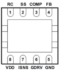
5 Pin Configuration and Functions
VSON (DRB) PACKAGE
8 PINS
(BOTTOM VIEW)
SOIC (D) PACKAGE
8 PINS
(TOP VIEW)
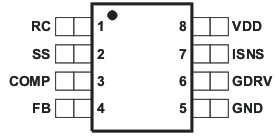
Pin Functions
| PIN | I/O | DESCRIPTION | |
|---|---|---|---|
| NAME | NO. | ||
| COMP | 3 | O | Error amplifier output. Connect control loop compensation network from COMP to FB. |
| FB | 4 | I | Error amplifier inverting input. Connect feedback resistor network center tap to this pin. |
| GND | 5 | Device ground. | |
| GDRV | 6 | O | Driver output for external P-channel MOSFET |
| ISNS | 7 | I | Current-sense comparator input. Connect a current sense resistor between ISNS and VDD in order to set desired overcurrent threshold. |
| RC | 1 | I | Switching frequency setting RC network. Connect a capacitor from the RC pin to the GND pin and connect a resistor from the VDD pin to the RC pin. The device may be synchronized to an external clock by connecting an open drain output to this pin and pulling it to GND. For mor info on pulse width for synchronization, please refer to the Synchronizing the Oscillator section. |
| SS | 2 | I | Soft-start programming pin. Connect capacitor from SS to GND to program soft start time. Pulling this pin below 150 mV causes the output switching to stop, placing the device in a shutdown state. The pin also functions as a restart timer for overcurrent events. |
| VDD | 8 | I | System input voltage. Connect local bypass capacitor from VDD to GND. |