SLUUCD1A April   2020  – April 2022 TPS62860


  1.   Trademarks
  2. 1Introduction
    1. 1.1 Background
    2. 1.2 Performance Specification
    3. 1.3 Modifications
      1. 1.3.1 IC U1 Operation
  3. 2Setup
    1. 2.1 Input and Output Connector Description
      1. 2.1.1  J1, Pin 1 and 2 – VIN
      2. 2.1.2  J1, Pin 3 and 4 – S+/S-
      3. 2.1.3  J1, Pin 5 and 6 – GND
      4. 2.1.4  J2, Pin 1 and 2 – VOUT
      5. 2.1.5  J2, Pin 3 and 4 – S+/S-
      6. 2.1.6  J2, Pin 5 and 6 – GND
      7. 2.1.7  JP1 – EN
      8. 2.1.8  JP3 – VSEL1
      9. 2.1.9  JP4 - VSEL2
      10. 2.1.10 JP5 – PG
    2. 2.2 Setup
  4. 3Board Layout
    1. 3.1 Layout
  5. 4Schematic and Bill of Materials
    1. 4.1 Schematic
    2. 4.2 Bill of Materials
  6. 5Revision History

Schematic

Figure 4-1 illustrates the EVM schematic.
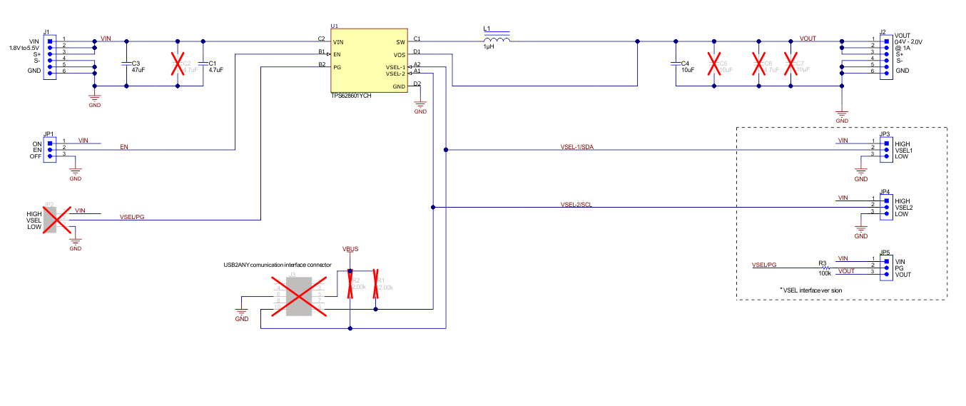
GUID-99C460DF-D10A-48E2-9809-CA0060BC7A20-low.gif Figure 4-1 TPS6286x1EVM Schematic