SLUUCJ2C july 2021 – august 2023
4.5 Probing the EVM
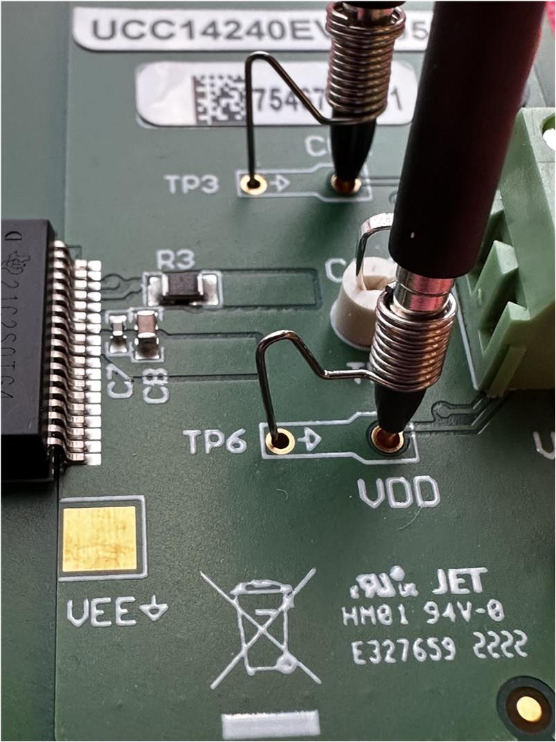
Using TP4, TP6 and TP10 oscilloscope probe PCB test points: The UCC12240-Q1 is a high frequency DC-DC module that requires careful measurement for accurately capturing transient events and measuring high frequency, AC ripple voltage. Remove the “witch hat” probe tip cover and ground lead from the scope probe. If scope probe ground springs are not available, wrap a piece of 22 AWG bare wire around the scope probe ground ring and insert the probe tip and ground into the EVM as shown in Figure 4-2.

Figure 4-2 UCC14240EVM-052, PCB Scope Probe Test Points
The EVM output nomenclature (VDD, VEE, COM) corresponds to what is commonly used when referring to isolated gate driver ICs. As shown in Figure 3-1, TP4 (COM) is the midpoint of a capacitive divider and is intended to connect to the COM pin of the isolated gate driver IC. When the UCC14240-Q1 is used to bias a gate driver IC, VDD (VDD-COM) and VEE (VEE-COM) are referred to with respect to COM. In this case consider COM as a virtual GND to the gate driver IC. Because the midpoint of the capacitive divider is sensitive to charge imbalance, do not connect any ground-referenced, test equipment to TP4 (COM) when probing the EVM. A battery powered DVM can be used to measure VEE with respect to COM. COM is therefore not be considered as GND but is really a sort of “virtual GND” to the gate driver IC. Since the midpoint of the capacitive divider is sensitive to charge imbalance, for the purpose of probing the EVM, do not to connect any ground-referenced, test equipment to TP4 (COM). A battery powered DVM can be used to measure VEE with respect to COM. When testing the EVM as a stand-alone bias power supply, oscilloscope probing of the secondary-side outputs is limited to TP3 and TP6 which are referenced to VEE. This means VDD displays an oscilloscope measurement of VDD+|VEE| and VEE displays |VEE|. Connecting any ground-referenced test equipment to COM can result in a “false” but safe overcurrent condition causing VDD and VEE to inadvertently drop out of regulation during light load operation.