SLVA857B July 2018 – January 2023 TPS50601-SP , TPS50601A-SP , TPS7H1101-SP , TPS7H1101A-SP , TPS7H3301-SP , TPS7H4001-SP
3.2 Setup
To demonstrate the applicability of TI’s space portfolio to this design, an RTG4 development kit was modified such that the voltage rails associated with power-up requirements were replaced with Evaluation Modules (EVM) ofour space qualified power devices (TPS50601SPEVM-S, TPS50601SPEVM-D and TPS7H1101SPEVM). This demonstration was set-up to show successful functionality under heavy load and due to limitations in which the demonstration was made, and does not exactly match with what is suggested for a grounds up design. The RTG4 was flashed with a high current design that resulted in a core current consumption of approximately 5 A at 1.2 V. The test setup can be seen in Figure 3-3.
 Figure 3-3 RTG4 Modified Development
Board Connected to TI Evaluation Modules
Figure 3-3 RTG4 Modified Development
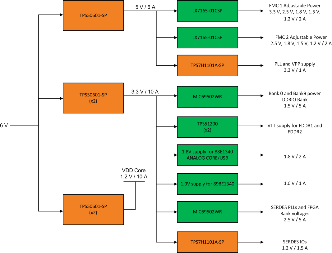
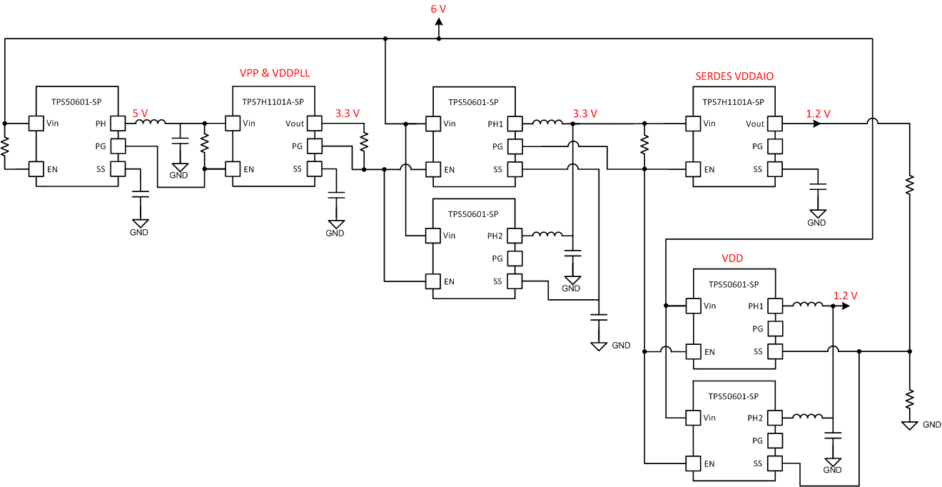
Board Connected to TI Evaluation ModulesThe reset supervisor on the development board was then removed and the voltage rails were sequenced using the power good and enable pins of each device as shown in Figure 3-5. The 12-V input source to the development board was changed to a 6-V source to satisfy the input requirements of the TI space power devices. The power tree for the modified development board is shown in Figure 3-4. The new components are shown in orange.
 Figure 3-4 RTG4 Modified Development
Board Power Distribution Using TI Space Qualified Components
 Figure 3-5 RTG4 Modified Development
Board Power Sequence
Figure 3-5 RTG4 Modified Development
Board Power SequenceThe rise times of all devices were configured to be at least 1 ms to avoid inrush currents. The core rail, VDD, is ratiometrically sequenced with the SERDES IO rail to ensure both voltage rails rise at the same time as required by the RTG4.