SLVAE09B July 2018 – August 2021 TPS560430
3.1 Inductor Design
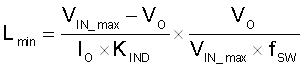
Equation 17 calculates the value of the output conductor. KIND is a coefficient that represents the amount of inductor ripple current relative to the maximum output current of the device. A reasonable value of KIND is 0.2 – 0.4. Since the ripple current increases with the input voltage, the maximum input voltage is used to calculate the minimum inductance LMIN, while KIND = 0.4 is selected. The minimum inductor value is calculated to be 16.3 μH. Choose the nearest standard inductor: L= 18 μH.
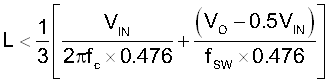
From Equation 12, the maximum inductor value is calculated to get enough phase margin. Three times margin is suggested and the limit is Equation 18 with the TPS560430 internal parameter. If you assume the target crossing over frequency fc is about 20 kHz, then the result is L < 40 μH at the minimum VIN. The selected 18-μH inductor meets the requirement.
The TPS560430 is protected from over-current conditions by the cycle-by-cycle current limit. To prevent inductor saturation in case of short circuit conditions, the inductor saturation current must be greater than the device maximum peak current limit, which is 1.4 A for the TPS560430.