SLVAE09B July   2018  – August 2021 TPS560430


  1.   Trademarks
  2. 1Introduction
  3. 2Peak Current Mode Loop Modeling
    1. 2.1 Overall Control Block Diagram and Transfer Function Derivation
    2. 2.2 Inside Current Loop Model
    3. 2.3 Overall Loop Model
    4. 2.4 Inductor and Output Capacitor Design Limits
    5. 2.5 The Equation to Calculate Bandwidth and Phase Margin
  4. 3Inductor and Output Capacitor Design
    1. 3.1 Inductor Design
    2. 3.2 Output Capacitor Design
    3. 3.3 Simulation and Bench Verification
  5. 4Summary
  6. 5References
  7. 6Revision History

The Equation to Calculate Bandwidth and Phase Margin

From Equation 11 and considering fc ≫ fP_OUT, fc ≫ fZ_EA, fc ≪ fP_EA, fc ≪ fP_ci, and fc ≪ fZ_OUT, the magnitude of open loop transfer function at crossover frequency fc is shown in Equation 14.

Equation 14. GUID-3A78527F-D3B4-4FF0-BDAA-395E6E541EF1-low.gif

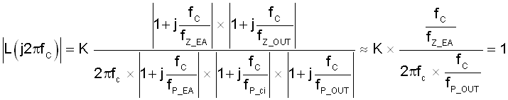
Considering RESR ≪ RO, the crossover frequency fc is obtained: Equation 15

Equation 15. GUID-994DF9DE-38E1-4F47-91AB-B6E669CDB722-low.gif

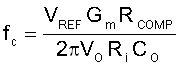
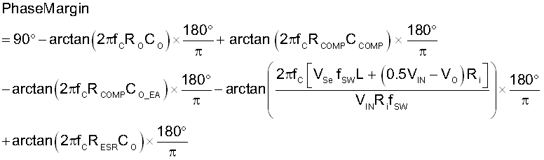
Phase margin is the phase of open loop transfer function at fc minus -180°: Equation 16

Equation 16. GUID-0D876D0D-0E3D-4443-A6F0-B334CB4EEDA3-low.gif