SLVAEP4 October 2023 BQ79600-Q1 , BQ79612-Q1 , BQ79614-Q1 , BQ79616 , BQ79616-Q1 , BQ79652-Q1 , BQ79654-Q1 , BQ79656-Q1
2 Receiver Topology and Common Mode Voltages
The daisy chain is bi-directional and half duplex, and, therefore, has a transmitter (TX) and receiver (RX) on the COMH and COML interfaces. The TX and RX functions are controlled automatically by the hardware based on the device’s base/stack detection. When a WAKE ping/tone is received, the communication direction is set by CONTROL1[DIR_SEL] and the COMM_CTRL[TOP_STACK] configurations. See Start Communication in the bq79616-Q1 data sheet for details. Additionally, a user overwrite to take over the complete control of the COMH and COML is available under communication debug mode using the DEBUG_CTRL_UNLOCK, DEBUG_COMM_CTRL1, and DEBUG_COMM_CTRL2 registers. See the Debug Control and Status section for more details in the bq79616-Q1 data sheet. Additionally, for a more detailed explanation of the basic timings and function of the protocol and plots below, visit section 9.5.1.2. of the bq79616-Q1 data sheet.
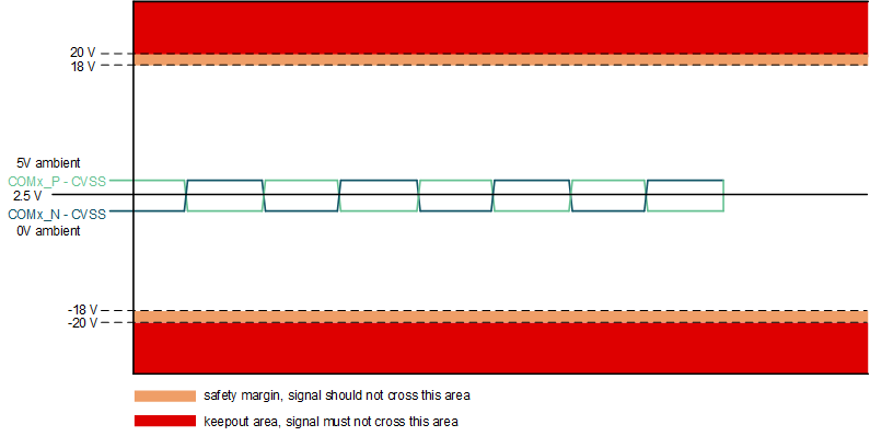
The RX topology of the bq7961X devices is similar to RS485 but with added design mechanisms to attenuate common mode voltages of up to ±20V due to noisy conditions. This common mode voltage limit for the differential signals is best explained by the chart in Figure 2-1. In an ambient test scenario, the common mode voltage of both the COM*P and COM*N holds at 2.5 V when there are no communications occurring. This is necessary because the attenuation of a negative signal would otherwise not bring the voltage between the receivers local ground and 5 V CVDD rail (internal LDO dedicated for communications). If communications occur, then the device will drive the COM pins with the CVDD rail between 0V (low) and 5V (high) and return to 2.5V between data packets (idle time) and after the communications have completed.
In the event of a common mode voltage swing due to noisy conditions such as EV inverter noise or Bulk Current Injection (BCI) testing – the common mode voltage seen at the COM pins may oscillate up to ±20 V depending on the isolation components and current injected. The device is designed to withstand this type noise level up to ±20 V because of the internal attenuation that allows the 5 V transceivers to handle the response and therefore the differential signal would still remain intact. Above this ±20 V level, there is risk of clamping the internal ESD structure or causing damage to the COM pins. This limit should be taken into consideration when determining BCI limits and testing.
 Figure 2-1 Common Mode Voltage Diagram