SLVAFC0 February 2022 TPS272C45
4 Surge Test Results
Surge tests have been performed on TPS272C45C to ensure the robustness of the device. The surge waveform demonstrated in Figure 4-1 follows the IEC61000-4-5 standard at 1 kV with 42 Ω impedance. The 42 Ω impedance represents the impedance between all other lines and GND IEC 61000-4-x Tests for TI’s Protection Devices application report.
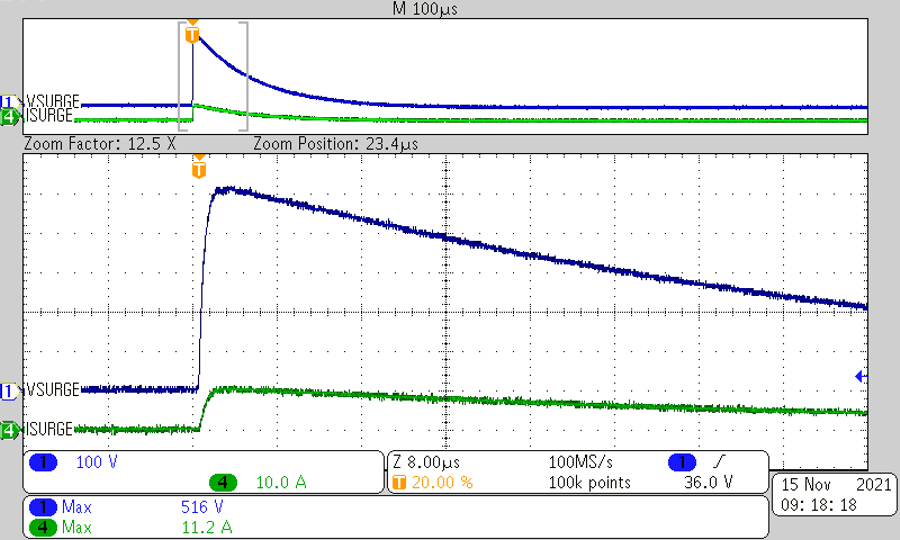 Figure 4-1 Surge Waveform on Resistive
Load
Figure 4-1 Surge Waveform on Resistive
LoadBoth positive and negative surges have been performed at VS and VOUT, and the two surge test setups are shown in Figure 4-2 and Figure 4-3.
At first, the positive surge is applied on 24-V VS with EN high for both channels and a 12 Ω load connected at the output. The waveform is shown in Figure 4-4. The VS is clamped by the VS to GND TVS diode D2 during the surge event, and it will absorb the majority of the surge energy. The device goes back to the normal operation after the surge.
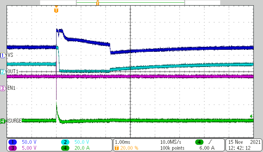 Figure 4-4 Waveform with Positive Surge Applied on VS
The second test involves a negative surge being applied to VS with the same setup. The resulting waveform is shown in Figure 4-5. In this case, the VS to GND diode D2 is conducting and keeping VS at the ground level during the negative surge. The device is operating as expected and kept on after the VS recovers.
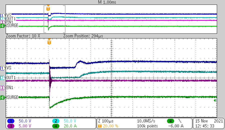 Figure 4-5 Waveform with Negative Surge Applied at VS
Turning now to the test setup demonstrated in Figure 4-3, surges are applied at VOUT with 24 V on the input, EN is high, and 12 Ω is connected to the load. Figure 4-6 shows the resulting waveform when the positive surge is applied. During the surge, the body diode will be conducting, and the diode from VS to GND will clamp the VS voltage. As current keeps flowing in the decoupling inductor, the voltage at Vs will remain high for a short duration and slowly recovers.
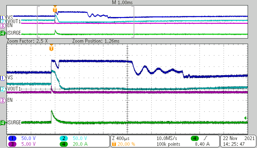 Figure 4-6 Waveform with Positive Surge Applied at VOUT and EN is High
Figure 4-7 shows the resulting waveform when the negative surge is applied to VOUT. The VS to GND TVS diode is conducting, which takes VS to the GND level. The supply and FET operation resumes normal operation after the surge pulse is over.
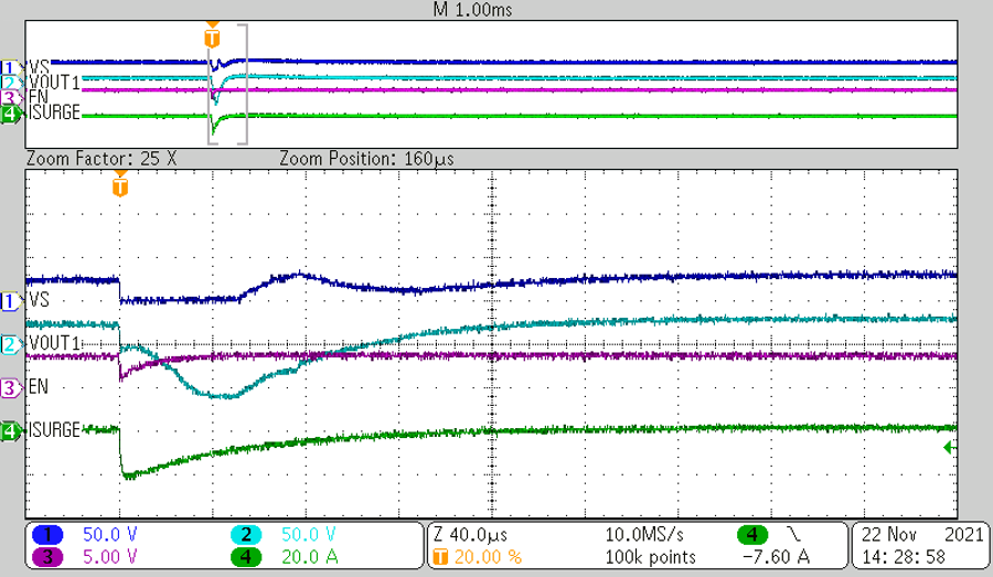 Figure 4-7 Waveform with Negative Surge Applied at VOUT and EN is High
The same surge tests are performed at VOUT while EN is low. With a positive surge at VOUT, Figure 4-8 shows that the TVS diode from VOUT to VS is conducting, and then VS voltage is clamped by the other TVS diode. The device is kept off after the surge event.
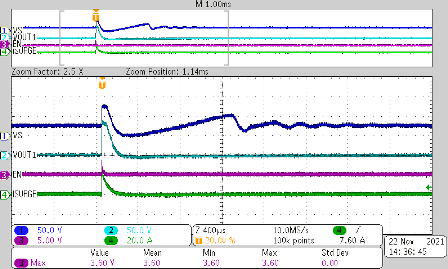 Figure 4-8 Waveform with Positive Surge Applied at VOUT and EN is Low
When the negative surge is applied at VOUT with EN low, Figure 4-9 shows the behavior where the VS to GND diode is conducting and the VS to VOUT diode is clamping. The device remains off after the surge pulse as expected.
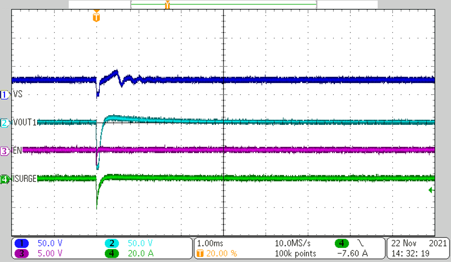 Figure 4-9 Waveform with Negative Surge Applied at VOUT and EN is Low