SLVAFK0 may 2023 LM7480-Q1 , LM74900-Q1
Introduction
Decentralized power distribution in zone architectures has led to multiple and redundant power supply inputs to zonal modules and power distribution boxes. One way to accommodate multiple supplies is to implement a power multiplexer (MUX). A power MUX is a circuit that selects between two or more power supplies to power a single output. This application brief discusses the implementation of a priority power MUX using the LM74800-Q1 ideal diode controller.
A priority power MUX automatically transitions the primary power supply to an auxiliary (AUX) or secondary power supply when the primary supply voltage drops below a designed threshold. When available and within acceptable limits, the primary power supply always has the highest priority to power the load. For example, if an upstream smart fuse trips on the primary power supply to a zonal module, then the priority power MUX circuit automatically connects the AUX supply to the output and disconnects the primary supply from the output to avoid any disruptions in the zonal module operation. If the upstream smart fuse is reset and the primary supply voltage rises above the designed threshold, then the priority power MUX circuit automatically connects the primary supply back to the output and disconnects the AUX supply.
The LM74800-Q1 drives back-to-back N-channel MOSFETs (FET) where the diode FET (QDIODE) blocks reverse current flow between the supplies and the load switch FET (QLOAD) disconnects the supply from the output. Each power rail uses a LM74800-Q1 to control external FETs and the outputs of each are connected together at the output node to power downstream loads such as DC/DC converters, LDOs, and so on. Figure 1 shows the block diagram for a priority power MUX using two LM74800-Q1 devices.
 Figure 1 Priority Power MUX Block Diagram With LM74800-Q1
Back-to-Back FET Topologies
LM74800-Q1 can drive FETs in two configurations: common drain (CD) and common source (CS). In CD topology, the drain terminals of both FETs are connected together as Figure 2 shows. When the LM74800-Q1 is in shutdown mode, the CD node can power critical always on loads through the body diode of Q1CD. When a reverse voltage is applied at the input, Q1CD turns off immediately, protects the CD node and loads at the output from being subjected to negative voltage. Since the CD node is always powered when the input voltage is positive, the VS pin can be directly connected to the CD node making the connections simple. The tradeoff for CD topology is that the CD node is always high due to the body diode of Q1CD even when the FET is turned off. As a result, it is not possible to check if Q1CD has failed short by measuring the voltage across the FET.
 Figure 2 Common Drain Topology
In CS topology, the source terminals of both FETs are connected together as Figure 3 shows. CS topology is specifically required in a few applications such as, Q1CS failed short detection and 200-V load dump protection. A voltage measurement can be taken across Q1CS to detect a failed short condition due to the body diode orientation. The CS node must only be equal to the input voltage when Q1CS is turned on. If the CS node voltage is high when Q1CS is turned off, then Q1CS is shorted between source and drain. If 200-V load dump protection is required, see the block diagram in LM7480-Q1 Ideal Diode Controller with Load Dump Protection. For the purpose of this application brief, assume only a suppressed load dump condition can occur.
 Figure 3 Common Source Topology
Priority Power MUX Design With LM74800-Q1
The priority power MUX circuit uses two power supplies: primary (VPRIM) as the main power supply and AUX (VAUX) as the backup or secondary supply. Figure 4 shows the schematic diagram for a priority power MUX using two LM74800-Q1 devices in CD topology and Figure 5 shows CS topology. CS topology requires additional diodes D2 (as described in previous section) and D4 in comparison to CD topology.
 Figure 4 Priority Power MUX in
CD
 Figure 5 Priority Power MUX in
CS
Figure 5 Priority Power MUX in
CSIn CD and CS topologies, both LM74800-Q1 devices must monitor VPRIM. U1 monitors VPRIM by setting the undervoltage (UVLO) threshold through the EN/UVLO pin and U2 monitors VPRIM by setting the overvoltage (OV) threshold through the OV pin which is connected to VPRIM through an internal switch that is enabled when EN/UVLO is on. The U2 OV threshold must be set to a voltage slightly above the U1 UVLO threshold so there is never a condition that both supplies are disconnected from the load.
When VPRIM is within the acceptable voltage range, U1 is enabled and drives FETs QLOAD-PRIM (Q2CD or Q1CS) and QDIODE-PRIM (Q1CD or Q2CS) on to connect VPRIM to the output. Meanwhile, U2 is in a OV condition because VPRIM is larger than the OV threshold voltage and QLOAD-AUX (Q4CD or Q3CS) is driven off to disconnect the AUX supply from the load. Since the output is supplied by VPRIM, U2 detects a reverse voltage and QDIODE-AUX (Q3CD or Q4CS) is driven off.
When VPRIM falls below the U1 UVLO and U2 OV threshold voltages, U1 drives QLOAD-PRIM off to disconnect the primary supply and U2 drives FETs QLOAD-AUX and QDIODE-AUX on to connect the AUX supply to the output. If VPRIM rises above the U1 UVLO and U2 OV threshold voltages, then U1 drives QLOAD-PRIM and QDIODE-PRIM on to reconnect the primary supply and U2 drives QLOAD-AUX and QDIODE-AUX off to disconnect the AUX supply from the output and prevent reverse current.
Both U1 and U2 have reverse current protection through QDIODE-PRIM and QDIODE-AUX in the condition that both power supplies are switched on through QLOAD-PRIM and QLOAD-AUX at the same time. If both supplies are switched on, the power MUX behaves as a diode OR and provides the larger of the two input voltages (primary or AUX). Additionally, if there is a condition that both VPRIM and VAUX are at the exact same voltage and have not exceeded the reverse voltage threshold range (-6.4 mV to -1.3 mV), the LM74800-Q1 sinks current through DGATE and turns off QDIODE-AUX to prevent keeping the FET on when no current is flowing through the FET.
In any power MUX system, the goal is to minimize the time when QLOAD-PRIM (primary supply switch) is turning OFF and the load is transitioning to power from VAUX that is QLOAD-AUX (AUX supply switch) is turning ON to reduce the time the load has no input power supply connected. To do so, decreasing the turn on time of QLOAD-AUX is required to turn ON fast. However, the HGATE pin can only source 66 μA of gate current to QLOAD-AUX. By connecting the emitter of Q5 to the gate of QLOAD-AUX, the gate source current can increase due to the Q5 connection through the collector to the CAP pin. Furthermore, the QLOAD-AUX gate source current can be tuned by changing the resistor value of R5. Additionally, D3 is implemented to provide a path around Q5 to turn off QLOAD-AUX.
Table 1 shows the conditions of each device and the status of the FETs for an example automotive application where VPRIM and VAUX are both nominal 12 V. For U1, the OV threshold is set to 16 V and the UVLO threshold is set to 8 V both dependent on VPRIM. For U2, the OV threshold is set to 8.1 V which is dependent on VPRIM, and UVLO threshold is set to 8.1 V dependent on VAUX.
| Primary Voltage Range | Primary LM74800-Q1 Status | Primary FET Status | AUX Voltage Range | AUX LM74800-Q1 Status | AUX FET Status | VOUT Supplied by |
|---|---|---|---|---|---|---|
| VPRIMARY > 16 V | OV | QLOAD-PRIM off, QDIODE-PRIM off | VAUX < 8.1 V | UVLO | QLOAD-AUX off, QDIODE-AUX off | None |
| VPRIMARY > 16 V | OV | QLOAD-PRIM off, QDIODE-PRIM off | VAUX > 8.1 V | OV | QLOAD-AUX off, QDIODE-AUX off | None |
| 8.1 V < VPRIMARY < 16 V | Normal | QLOAD-PRIM on, QDIODE on | VAUX < 8.1 V | UVLO | QLOAD-AUX off, QDIODE-AUX off | VPRIMARY |
| 8.1 V < VPRIMARY < 16 V | Normal | QLOAD-PRIM on, QDIODE-PRIM on | VAUX > 8.1 V | OV and QDIODE blocks | QLOAD-AUX off, QDIODE-AUX off | VPRIMARY |
| 8 V < VPRIMARY < 8.1 V | Normal | QLOAD-PRIM on, QDIODE-PRIM on | VAUX < 8.1 V | UVLO | QLOAD-AUX off, QDIODE-AUX off | VPRIMARY |
| 8 V < VPRIMARY < 8.1 V | QDIODE Blocks | QLOAD-PRIM on, QDIODE-PRIM off | VAUX > 8.1 V | Normal | QLOAD-AUX on, QDIODE-AUX on | VAUX |
| VPRIMARY < 8 V | UVLO | QLOAD-PRIM off, QDIODE-PRIM off | VAUX < 8.1 V | UVLO | QLOAD-AUX off, QDIODE-AUX off | None |
| VPRIMARY < 8 V | UVLO | QLOAD-PRIM off, QDIODE-PRIM off | VAUX > 8.1 V | Normal | QLOAD-AUX on, QDIODE-AUX on | VAUX |
Test Results
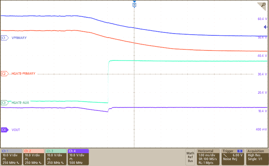
A test board was created to demonstrate the functionality of the priority power MUX circuit using LM74800-Q1 in CS topology. Figure 6 shows the waveforms for the primary supply, HGATE of primary, HGATE of AUX, and the output voltage (VOUT) when the primary supply turns off. When the voltage on the primary supply turns off, then HGATE AUX turns on before HGATE primary turns off. The output voltage drop is only minimal due to the fast transition from primary to AUX supply.
 Figure 6 Primary Supply Falling
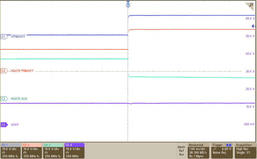
Figure 7 shows the waveforms for the primary supply, HGATE of primary, HGATE of AUX, and the output voltage (VOUT) when the primary supply turns on. When the voltage on the primary supply turns on, then HGATE primary turns on before HGATE AUX turns off. The voltage on VOUT remains stable during this transition.
 Figure 7 Primary Supply Rising
Priority Power MUX With Overcurrent (OC) Protection
The priority power MUX using LM74800-Q1 can also support overcurrent protection in a common source topology by adding an external current sense amplifier to the system. A current sense amplifier, such as the INA300-Q1, is recommended because the device can latch off the supply voltage when overcurrent is detected by pulling the EN/UVLO low to turn off the external FETs connecting to the LM74800-Q1 device. Each supply implements a current sense amplifier to monitor the individual supply current. Note that an additional wide input voltage LDO is required if an always on rail is not already available in the system. Figure 8 shows the block diagram including INA300-Q1.
 Figure 8 Priority Power MUX With
LM74800-Q1 and INA300-Q1 in CS
Figure 8 Priority Power MUX With
LM74800-Q1 and INA300-Q1 in CSIf a common drain topology is preferred, the LM74900-Q1 can replace the LM74800-Q1 in the priority power MUX circuit. The LM74900-Q1 features integrated overcurrent protection removing the need for an external current sense, which saves cost and space. Figure 9 shows the block diagram using LM74900-Q1.
 Figure 9 Priority Power MUX With
LM74900-Q1
Figure 9 Priority Power MUX With
LM74900-Q1Conclusion
A priority power MUX is used to switch between the primary supply and the AUX supply depending on the voltage level of the primary supply. LM74800-Q1 is used in a priority power MUX application and the back-to-back FETs are configured in common source or common drain topology. If overcurrent protection is required in the application, an additional current sense amplifier is added to the LM74800-Q1 priority power MUX design or LM74800-Q1 is replaced with LM74900-Q1 due to integrated over current protection and short circuit protection, but this device can only be used in common drain topology.