SLVU382A August   2010  – September 2021 TPS54425


  1.   Trademarks
  2. 1Introduction
  3. 2Performance Specification Summary
  4. 3Modifications
    1. 3.1 Output Voltage Setpoint
  5. 4Test Setup and Results
    1. 4.1 Input/Output Connections
    2. 4.2 Start-Up Procedure
    3. 4.3 Efficiency
    4. 4.4 Load Regulation
    5. 4.5 Line Regulation
    6. 4.6 Load Transient Response
    7. 4.7 Output Voltage Ripple
    8. 4.8 Input Voltage Ripple
    9. 4.9 Start-Up
  6. 5Board Layout
    1. 5.1 Layout
  7. 6Schematic, Bill of Materials, and Reference
    1. 6.1 Schematic
    2. 6.2 Bill of Materials
    3. 6.3 Reference
  8. 7Revision History

Schematic

Figure 6-1 is the schematic for the TPS54425EVM-538.
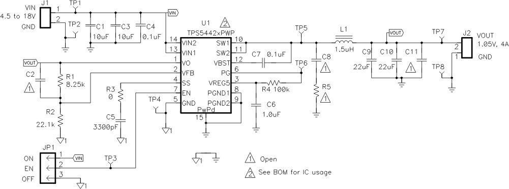
GUID-45DF9F93-2133-4647-82F2-3E836FBD4383-low.gifFigure 6-1 TPS54425EVM-608 Schematic Diagram