SLVU392A July 2010 – January 2022 TPS53125
- Trademarks
- 1Description
- 2TPS53125EVM-599 Electrical Performance Specifications
- 3TPS53125EVM-599 Schematic
-
4Connector and Test Point Descriptions
- 4.1 Enable Jumpers/Switches – SW1 and SW2
- 4.2
Test Point Descriptions
- 4.2.1 Input Voltage Monitoring – TPS and TP9
- 4.2.2 Channel 1 Output Voltage Monitoring – TP4 and TP8 or CN1
- 4.2.3 Channel 2 Output Voltage Monitoring – TP6 and TP7 or CN2
- 4.2.4 Soft-Start Voltage Monitoring – TP1, TP2, and TP3
- 4.2.5 Switching Node Monitoring – TP3, TP5, and TP11
- 4.2.6 5-V Regulator Output Monitoring – TP3 and TP10
- 5Test Setup
- 6TPS53125EVM-599 Test Data
- 7TPS53125EVM-599 Assembly Drawings and Layout
- 8TPS53125EVM-599 Bill of Materials
- 9Revision History
7 TPS53125EVM-599 Assembly Drawings and Layout
Figure 7-1 through Figure 7-5 show the design of the TPS53125EVM-599 printed-circuit board. The EVM has been designed using a 4-layer, 2-oz copper-clad circuit board 3.5 in 2.7 to allow the user to easily view, probe, and evaluate the TPS53125 control IC in a practical application. Moving components to both sides of the PCB or using additional internal layers can offer additional size reduction for space-constrained systems.
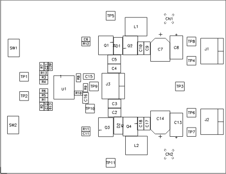 Figure 7-1 TPS53125EVM-599 Component Placement, Viewed From Top
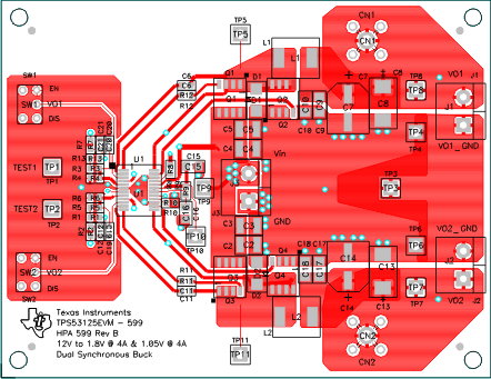 Figure 7-2 TPS53125EVM-599 Top Copper, Viewed From Top
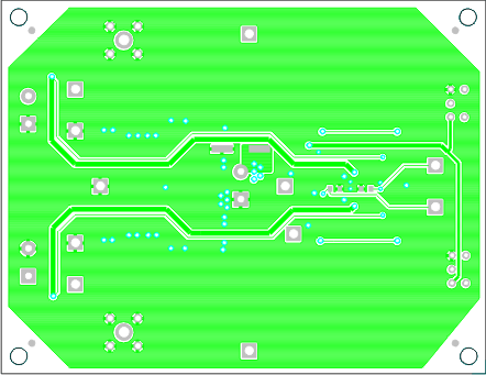 Figure 7-3 TPS53125EVM-599 Bottom Copper, Viewed From Bottom
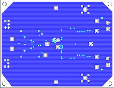 Figure 7-4 TPS53125EVM-599 Internal 1, X-Ray View From Top
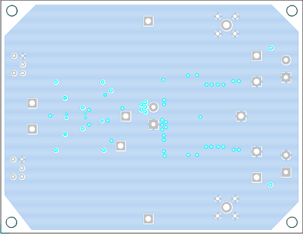 Figure 7-5 TPS53125EVM-599 Internal 2, X-Ray View From Top