SLVU793A October 2012 – June 2021 TPS56921
3.1 Layout
The board layout for the TPS56921EVM-188 is shown in Figure 3-1 through Figure 3-5. The top-side layer of the EVM is laid out in a manner typical of a user application. The top, bottom, and internal layers are 2-oz. copper.
The top layer contains the main power traces for PVIN, VIN, VOUT, and VPHASE. Also on the top layer are connections for the remaining pins of the TPS56921 and a large area filled with ground. The internal layer-1 is dedicated to a power ground plane. the internal layer-2 contains an analog ground fill area. This analog ground is used as a return for the I2C interface as well as for sensitive analog circuits for RT, SS, EN, COMP and VSENSE. The analog ground is connected to the main power ground at one place to inhibit circulating currents. This connection is made at the via near TP7. Internal layer-2 also contains additional fill areas for PVIN and VOUT, as well as connections to the I2C interface connector at J3. The bottom layer contains a power ground plane only. The top-side ground traces are connected to the bottom and internal ground planes with multiple vias placed around the board including nine vias directly under the TPS56921 and 12 vias directly adjacent to the TPS56921device to provide a thermal path from the top-side ground area to the internal layer-1 and bottom-side ground planes.
The input decoupling capacitors (C1,C2, C3 and C4) and bootstrap capacitor (C8) are all located as close to the IC as possible. Additionally, the voltage setpoint resistor divider components are kept close to the IC. The voltage divider network ties to the output voltage at the point of regulation, the copper VOUT trace at the J4 output connector. For the TPS56921, an additional input bulk capacitor may be required, depending on the EVM connection to the input supply.
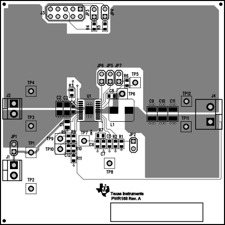 Figure 3-1 TPS56921EVM-188 Top-Side Assembly
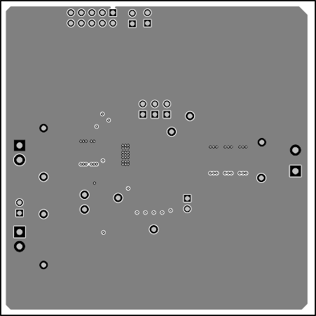 Figure 3-3 TPS56921EVM-188 Internal Layer-1 Layout
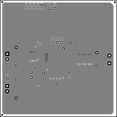 Figure 3-5 TPS56921EVM-188 Bottom-Side Layout
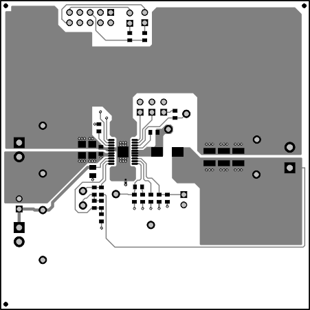 Figure 3-2 TPS56921EVM-188 Top-Side Layout
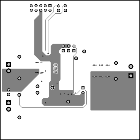 Figure 3-4 TPS56921EVM-188 Internal Layer-2 Layout