SLVUB26D May 2017 – February 2022 TPSM846C23
8 PCB Layout
Figure 8-1 through Figure 8-8 illustrate the EVM PCB layout images.
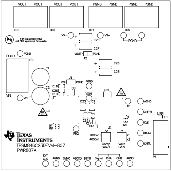 Figure 8-1 Top Components
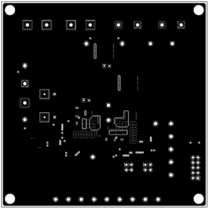 Figure 8-3 Layer 2 Copper
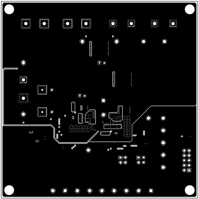 Figure 8-5 Layer 4 Copper
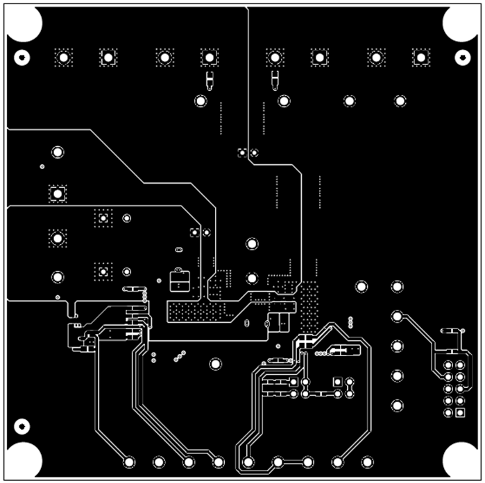 Figure 8-7 Bottom-Side Copper
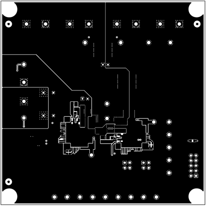 Figure 8-2 Topside Copper
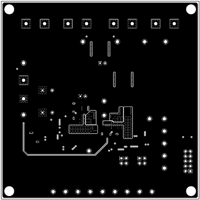 Figure 8-4 Layer 3 Copper
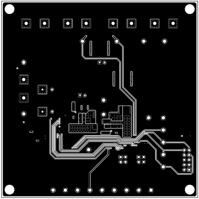 Figure 8-6 Layer 5 Copper
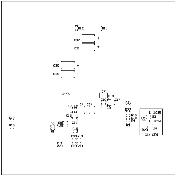 Figure 8-8 Bottom Components