SLVUB62B June 2017 – November 2020
- Trademarks
- 1 About this Manual
- 2 Information About Cautions and Warnings
- 3 Items Required for Operation
- 4 Introduction
-
5 Setup
- 5.1
Switch, Push Button, Connector, and Test Point Descriptions
- 5.1.1 Power Path Jumper Configuration
- 5.1.2 DP Source Receptacle
- 5.1.3 S1 HRESET Push-Button
- 5.1.4 S6 SPI MISO Pull Down Button
- 5.1.5 S3: FTDI Enable and Disable
- 5.1.6 S2: SPI , I2C, and BusPowerZ Configurations
- 5.1.7 J1: Barrel Jack Power Connector
- 5.1.8 Barrel Jack Detect
- 5.1.9 USB Type B Connector (J11)
- 5.1.10 USB Type-CConnector (J2)
- 5.1.11 USB Micro B Connector (J9)
- 5.1.12 TP13 (5 V), TP8 (3.3 V), and TP12 (1.2 V)
- 5.1.13 Aardvark Connector (J10)
- 5.1.14 TP10, TP11, TP15, TP16, TP17, TP18, TP9: GND Test Points
- 5.1.15 TP1, TP2, TP3 and TP4 – CC1 and CC2 Test Points
- 5.1.16 TP14 (PA and PB): VBUS Test Point
- 5.1.17 TP7, TP6, and TP5: A-VAR, B-VAR, and System Power Test Points Respectively
- 5.1.18 J3 and J4 (Bottom of EVM): Signal Headers
- 5.2 LED Indicators Description
- 5.1
Switch, Push Button, Connector, and Test Point Descriptions
- 6 Using the TPS65988EVM
- 7 Connecting the EVM
- 8 REACH Compliance
- 9 TPS65988EVM Schematic
- 10TPS65988EVM Board Layout
- 11TPS65988EVM Bill of Materials
- 12Revision History
9 TPS65988EVM Schematic
Figure 9-1 shows the block diagram of the main components of the TPS65988EVM. The main schematic blocks port A/B control MUX and SS MUX, USB HUB, power paths, power supplies, USB Type-C receptacles, processor, BoosterPack headers, and hardware.
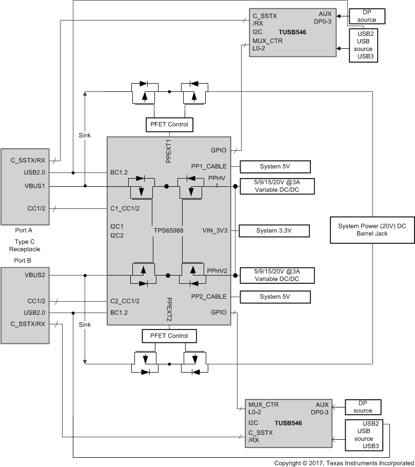 Figure 9-1 TPS65988EVM Block Diagram
Figure 9-2 illustrates the processor block showing the USB Type-C PD controller and contains connections for GPIOs, D+ and D-, CC1 and CC2, HRESET, I2C lines, SPI for flash memory, and ADC1 and ADC2.
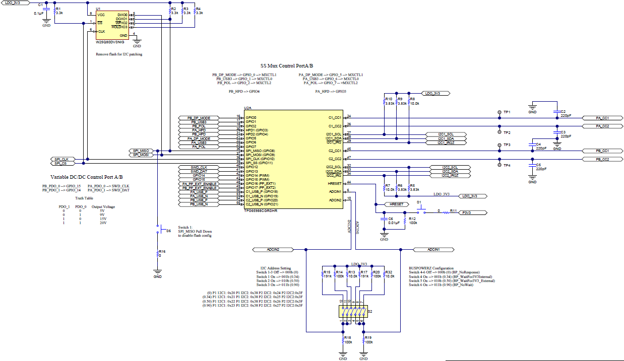 Figure 9-2 TPS65988EVM Processor Block
Figure 9-3 shows the power path block, which contains the power portion of the TPS65988 and the required passives. The external power path consists of back-to-back PMOS with RCP circuit. The internal power path is used for sourcing power and the external power path is used for sinking power. The TPS65988 power path can provide power to VBUS or consume power from VBUS.
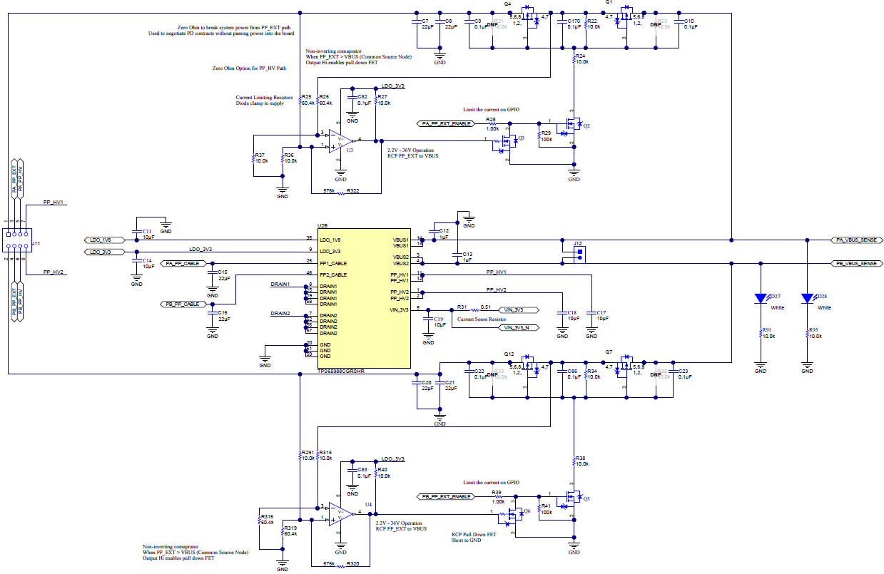 Figure 9-3 TPS65988EVM Power Path Block
Figure 9-4 shows the power supply block, which has all of the onboard supplies generated and the comparator circuit for barrel-jack detection. There are two variable supplies that generate 5, 9, 15, and 20 V. There are three DC/DC converters that generate 1.2, 3.3, and 5 V. The minimum voltage for SYS_PWR is 5 V; however, this also decreases VBUS maximum power capabilities. When using a lower voltage, the comparator circuit may have to be adjusted to trip at a lower voltage for proper barrel jack detection.
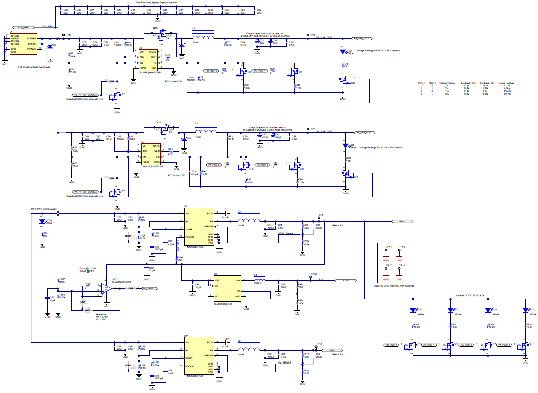 Figure 9-4 TPS65988EVM Power Supply Block
Figure 9-5 shows the DisplayPort Mux used to switch the DisplayPort signals to either USB Type-C Port.
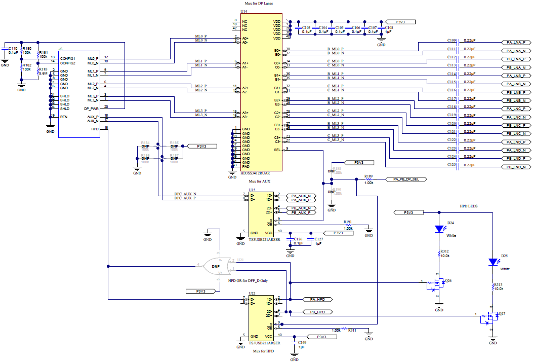 Figure 9-5 TPS65988EVM DisplayPort Mux
Figure 9-6 shows the SS MUX block for port A which connects the DP and USB signals from the DP and USB receptacle. Operating from the system 3.3-V rail, the SS MUX is used for configurations C, D, and E from DisplayPort. Achieve configurations through GPIO or I2C. As the host, the SS MUX is capable of USB 3.1 data rates up to 5 Gbps and DP 1.4 up to 8.1 Gbps with 2 or 4 DP lanes.
 Figure 9-6 TPS65988EVM SS MUX Block Port A
Figure 9-7 shows the SS MUX block for port B which connects the DP and USB signals from the DP and USB receptacle. Operating from the system 3.3-V rail, the SS MUX is used for configurations C, D, and E from DisplayPort. Achieve configurations through GPIO or I2C. As the host, the SS MUX is capable of USB 3.1 data rates up to 5 Gbps and DP 1.4 up to 8.1 Gbps with 2 or 4 DP lanes.
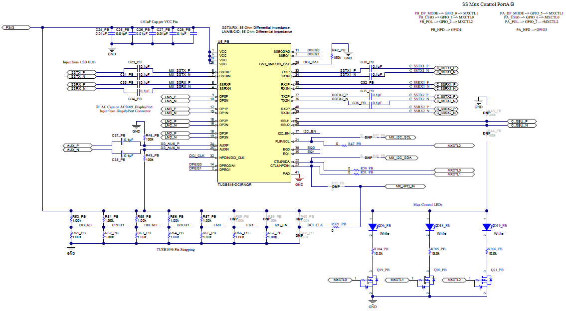 Figure 9-7 TPS65988EVM SS MUX Block Port B
Figure 9-8 shows the USB HUB, which contains the connections from the USB source receptacle.
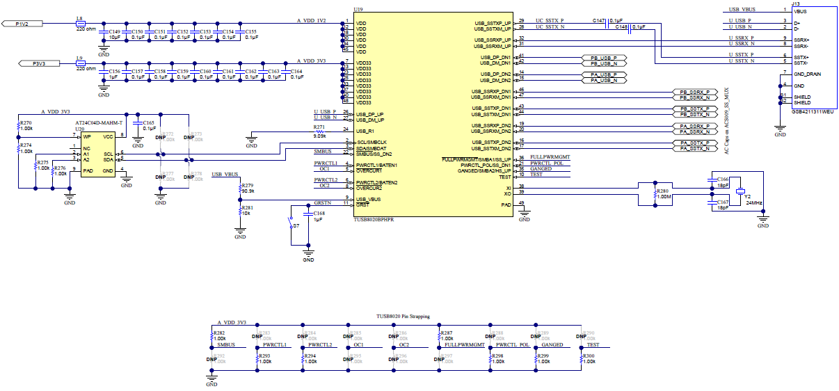 Figure 9-8 TPS65988EVM USB HUB
Figure 9-9 shows the USB Type-C block, which includes the USB Type-C port A and ESD protection.
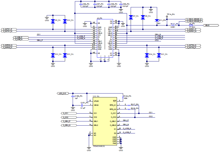 Figure 9-9 TPS65988EVM
USB Type-C™ Port-A Block
Figure 9-10 shows the USB Type-C block, which includes the USB Type-C port B and ESD protection.
 Figure 9-10 TPS65988EVM
USB Type-C™ Port B Block
Figure 9-11 shows the FTDI block, which contain the connections from the FTDI board.
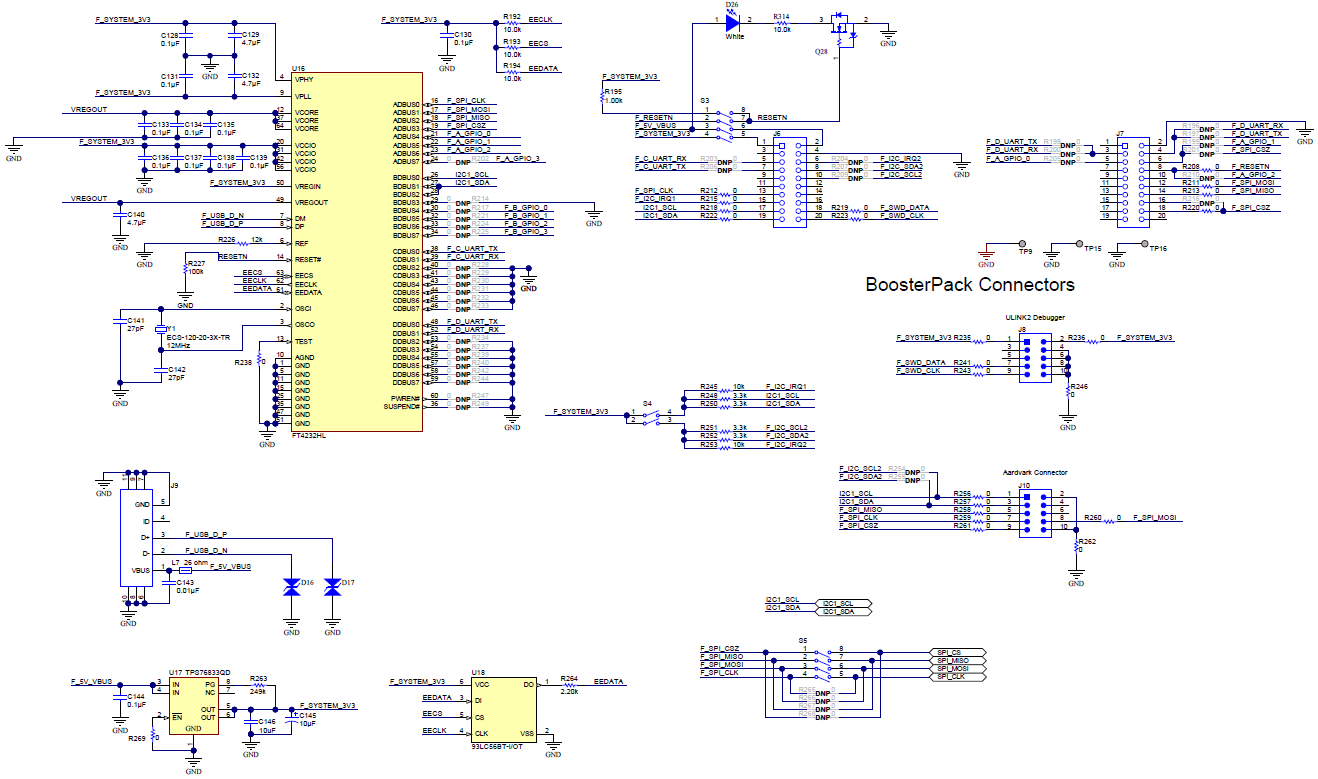 Figure 9-11 TPS65988EVM
FTDI® Connector Block
Figure 9-11 TPS65988EVM
FTDI® Connector BlockFigure 9-12 and Figure 9-13 show the current sense block, which contain the sense connections to VBUS and VIN_3V3 for port A and port B.
 Figure 9-12 TPS65988EVM Current Sense Block Port A
 Figure 9-13 TPS65988EVM Current Sense Block Port B
Figure 9-14 shows the BoosterPack headers block, which contain the connections to the BoosterPack headers.
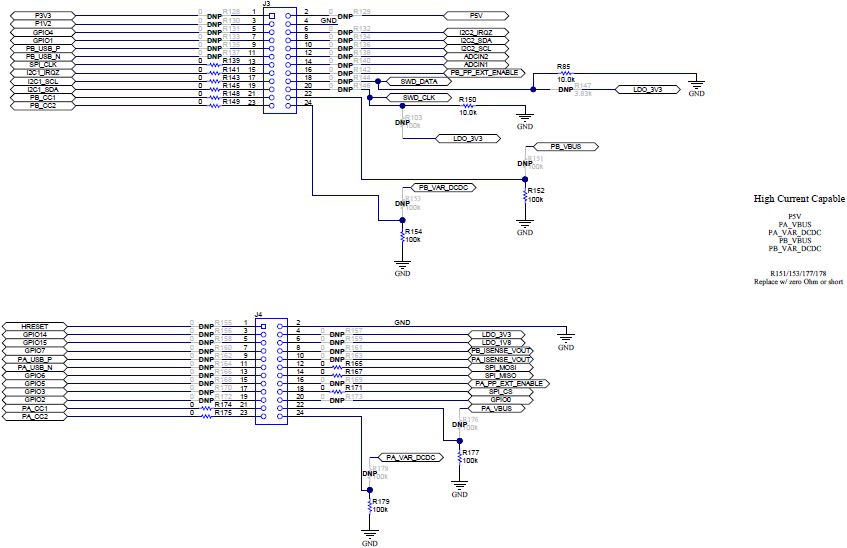 Figure 9-14 TPS65988EVM BoosterPack Header Block