SLVUBZ2A September 2020 – December 2020 LM5127-Q1
6.2 PCB Layers
Figure 6-3 through Figure 6-10 illustrate the EVM PCB layout images. 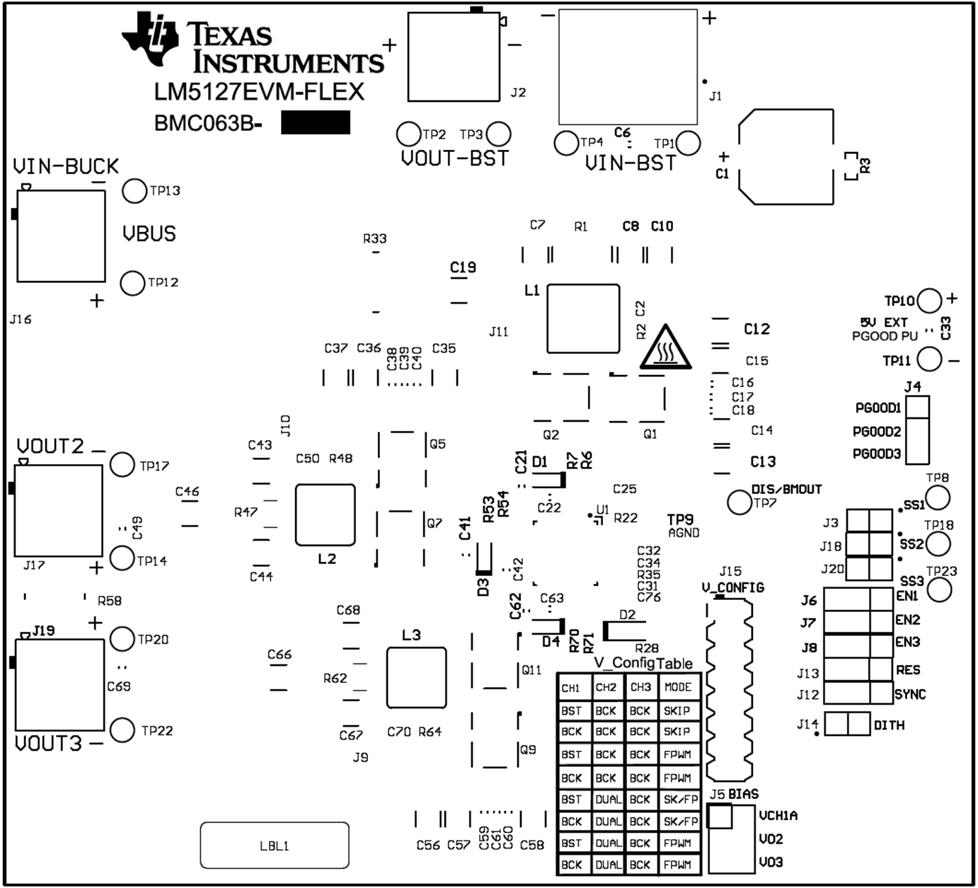 Figure 6-3 Layout: Top Silk Screen
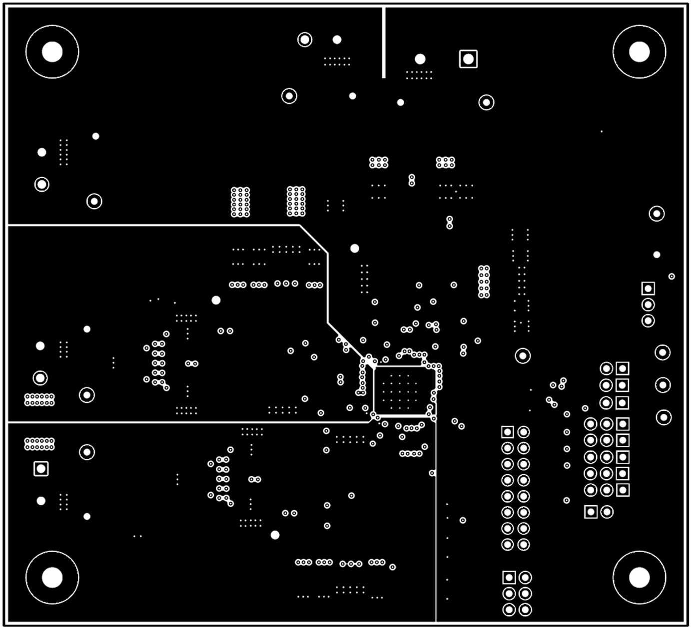 Figure 6-5 Layout: Signal Layer 1
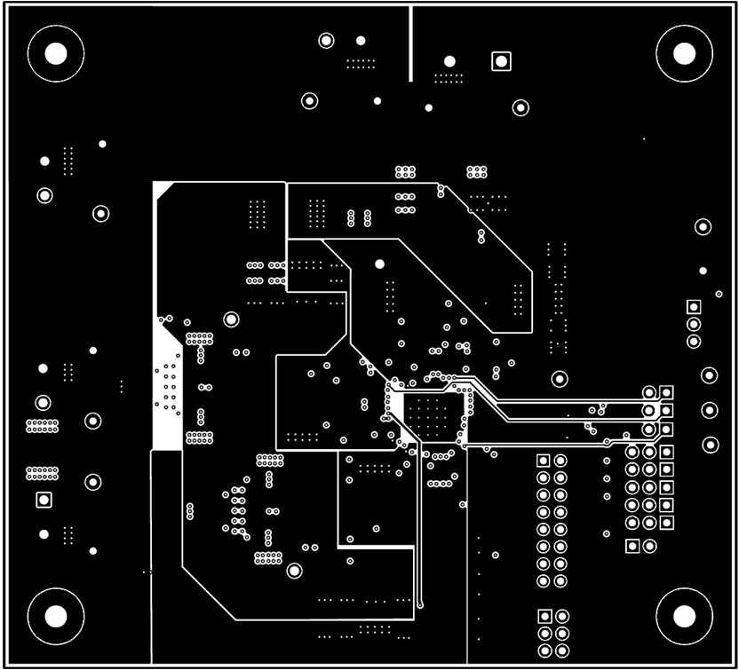 Figure 6-7 Layout: Signal Layer 3
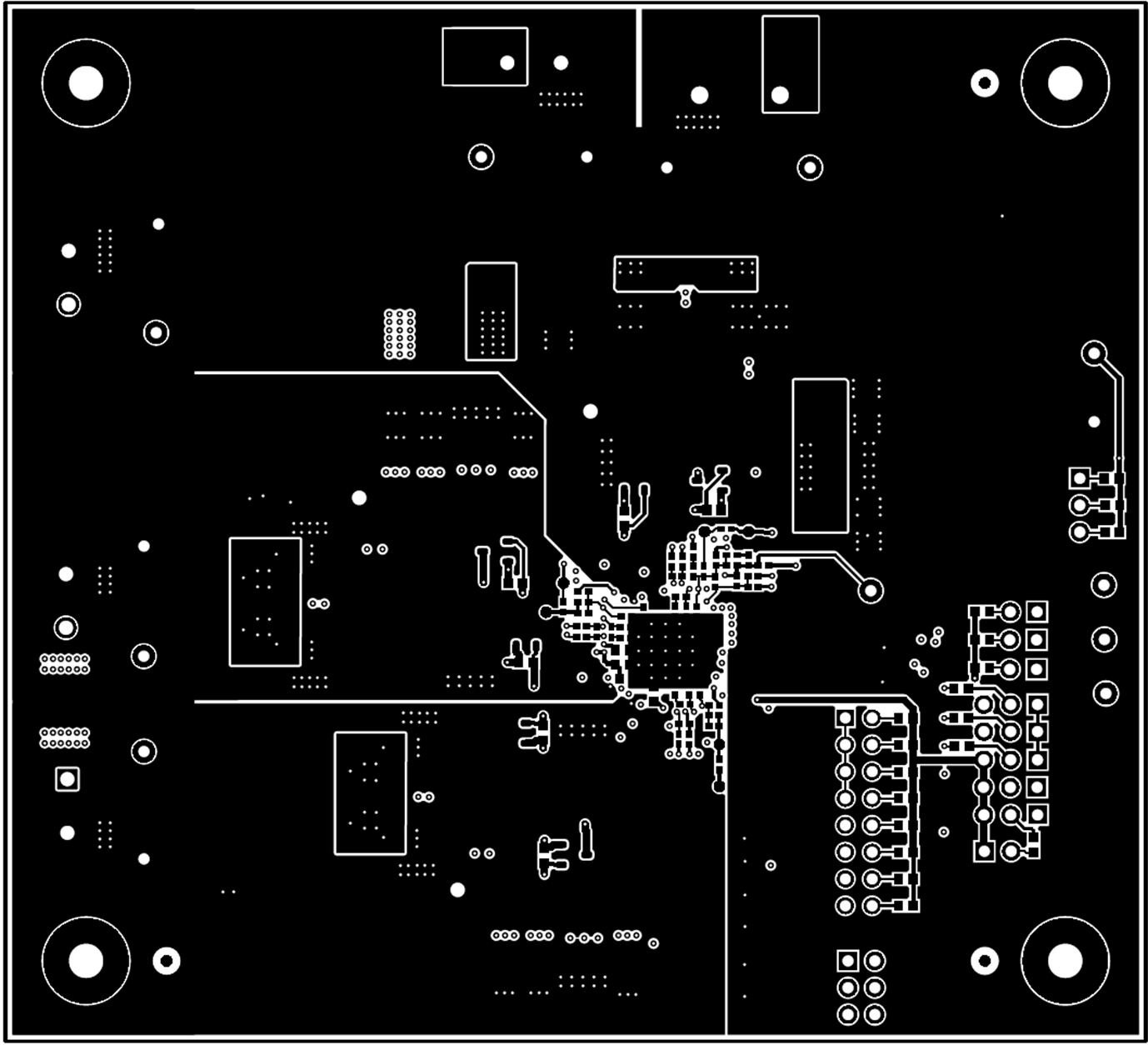 Figure 6-9 Layout: Bottom Layer
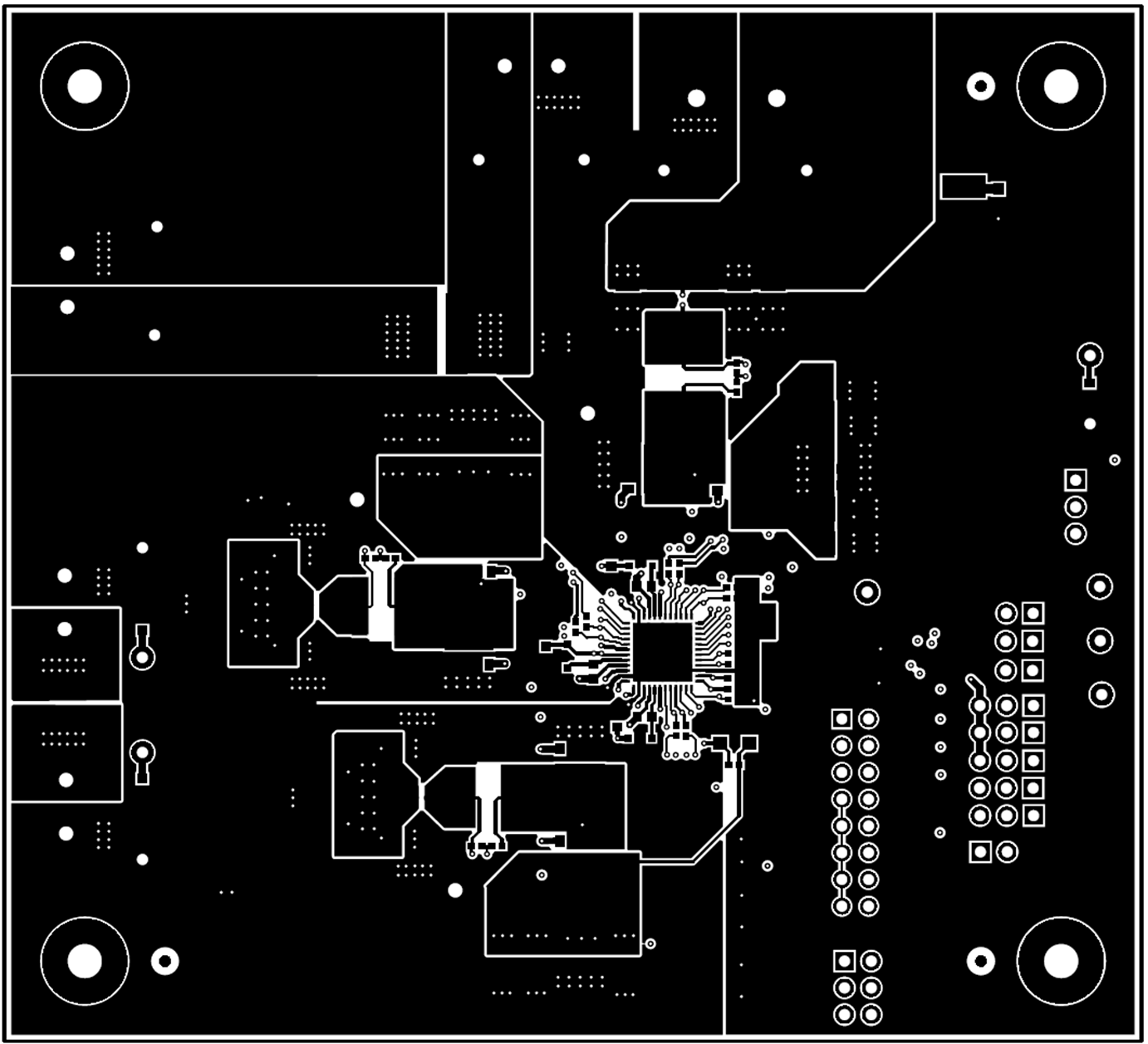 Figure 6-4 Layout: Top Layer
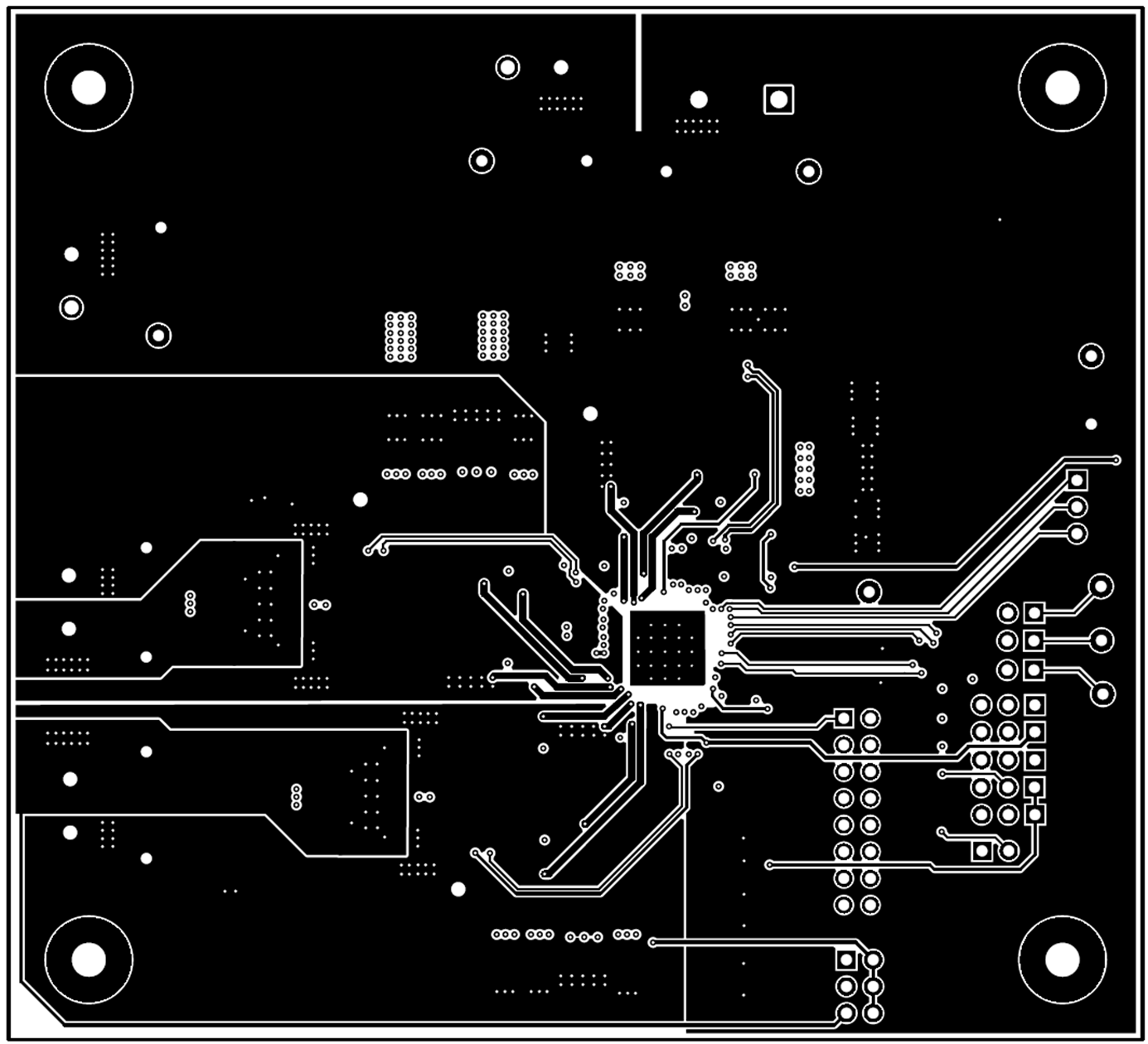 Figure 6-6 Layout: Signal Layer 2
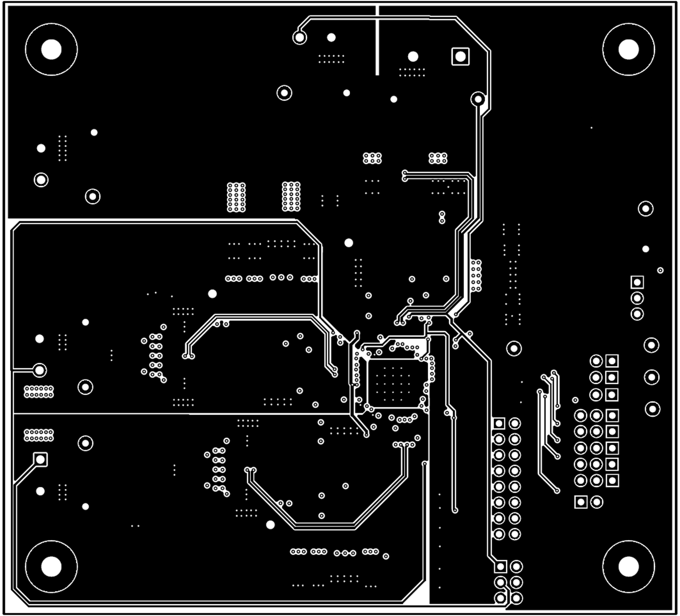 Figure 6-8 Layout: Signal Layer 4
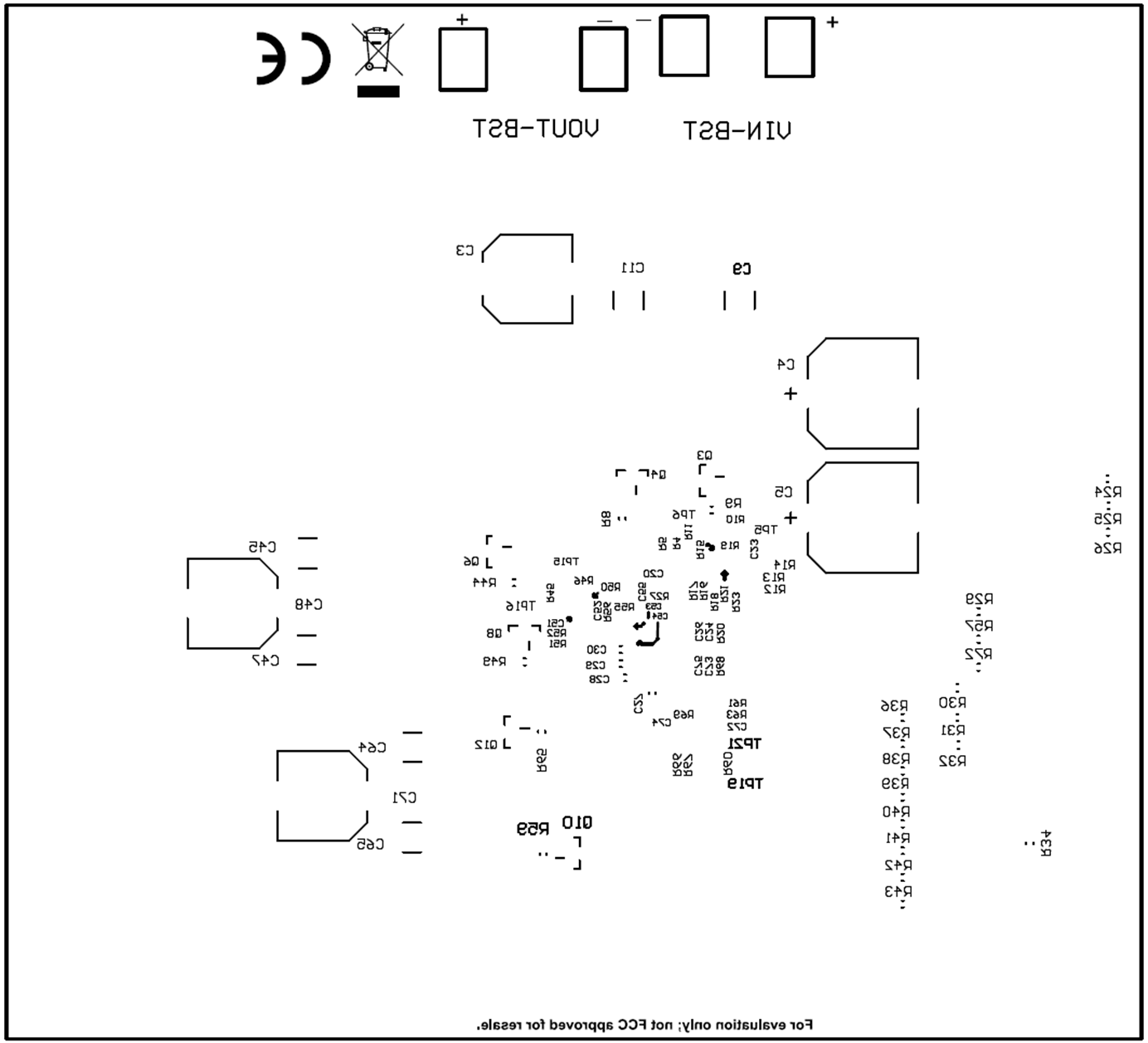 Figure 6-10 Layout: Bottom Silk Screen
 Figure 6-3 Layout: Top Silk Screen
 Figure 6-5 Layout: Signal Layer 1
 Figure 6-7 Layout: Signal Layer 3
 Figure 6-9 Layout: Bottom Layer
 Figure 6-4 Layout: Top Layer
 Figure 6-6 Layout: Signal Layer 2
 Figure 6-8 Layout: Signal Layer 4
 Figure 6-10 Layout: Bottom Silk Screen