SLVUC03 November 2022 TPS25762-Q1 , TPS25772-Q1
7 Board Views and Layout Prints
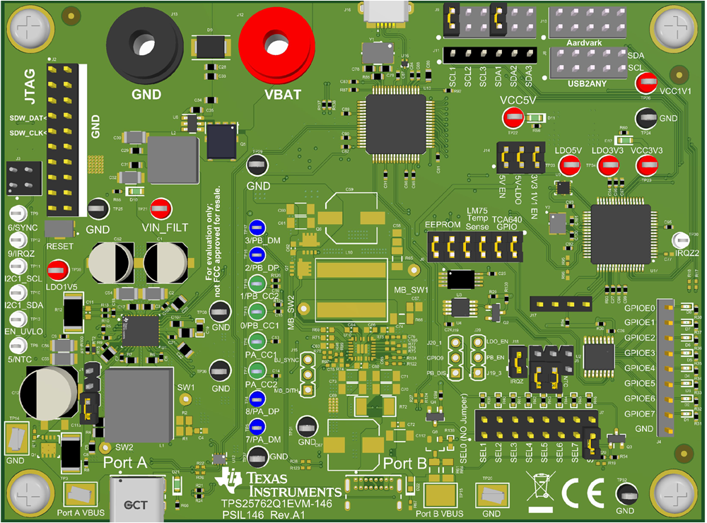
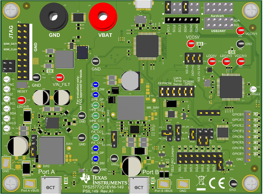
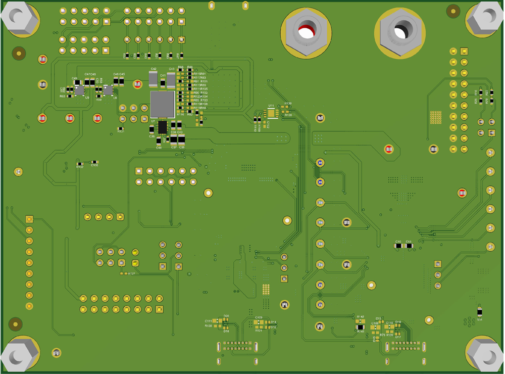
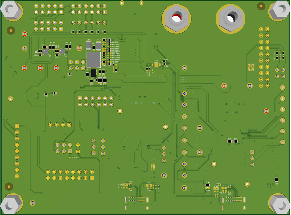
TPS25762EVM-146, TPS25772Q1EVM-149, and TPS25772Q1EVM-150 have the same PCB layout. Figure 7-1, Figure 7-2, Figure 7-3, Figure 7-4 show the PCB layouts of the EVM. Figure 7-5 and Figure 7-6 show the 3D top and bottom view for TPS25762Q1EVM-146, Figure 7-7 and Figure 7-8 show the 3D top and bottom view for TPS25772Q1EVM-149, Figure 7-9 and Figure 7-10 show the 3D top and bottom view for TPS25772Q1EVM-150.
Figure 7-1 Top Layer
Figure 7-2 Middle Layer1
Figure 7-3 Middle Layer2
Figure 7-4 Bottom Layer
 Figure 7-5 TPS25762Q1EVM-146 3D Top View
 Figure 7-6 TPS25762Q1EVM-146 3D Bottom View
 Figure 7-7 TPS25772Q1EVM-149 3D Top View
 Figure 7-8 TPS25772Q1EVM-149 3D Bottom View
 Figure 7-9 TPS25772Q1EVM-150 3D Top View
 Figure 7-10 TPS25772Q1EVM-150 3D Bottom View