SLVUCD0 February 2022 TPS7H5002-SP , TPS7H5003-SP , TPS7H5004-SP
2 EVM Setup and Quick Start Guide
Default EVM Configuration lists the default configuration.
| Parameter | Specification |
|---|---|
| Input Power Supply | 4 V to 14 V |
| Operating Temperature | 25°C |
| Switching Frequency | 500 kHz |
The TPS7H5001/2/3/4EVM-CVAL can be quickly turned on and run using the connections shown in TPS7H5001EVM-CVAL Connections.
| Terminal or Test Point | Voltage Source |
|---|---|
J11 (VIN) | 4 to 14-V input at 10 mA. See Positive and Negative Terminal for J11 for connections. |
TP9 (COMP) | 1 V at < 10 mA (input range can be –0.3 V to 3.3 V based on the TPS7H5001-SP Radiation-Hardness-Assured Si and GaN Dual Output Controller data sheet) |
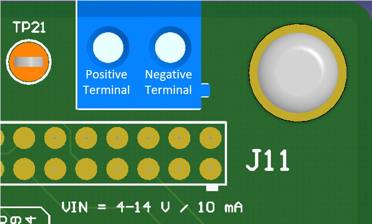
Positive and Negative Terminal for J11 shows which terminal is the positive and negative on J11. Connect the positive input voltage to the positive terminal and GND to negative terminal.
 Figure 2-1 Positive and Negative Terminal for J11
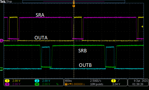
The device then turns on and operates in open loop mode as shown in TPS7H5001-SP Output. TPS7H5001-SP Output shows the output of TPS7H5001-SP measured on J1–J4 with the quick start method.
 Figure 2-2 TPS7H5001/2/3/4-SP Output
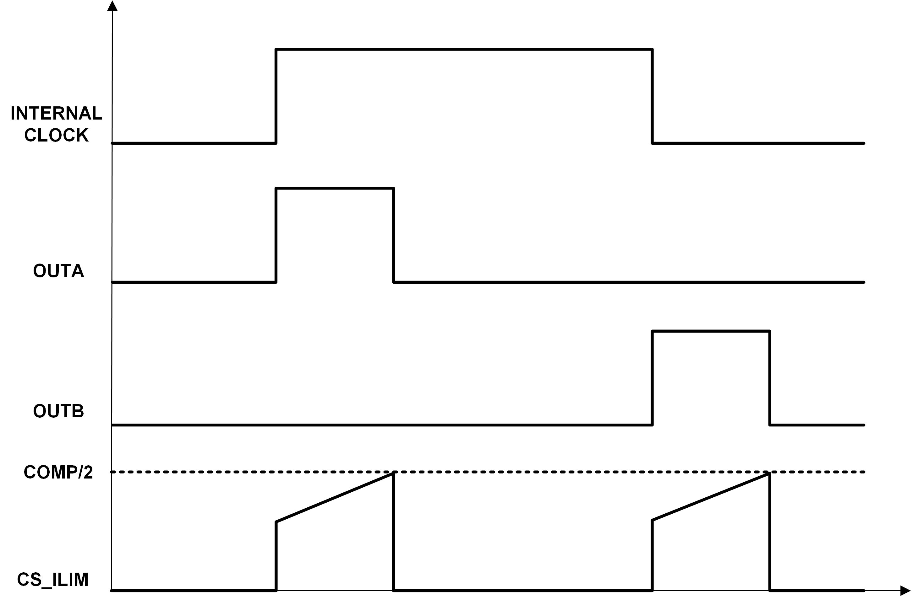
The operation of this mode is such that forcing the voltage on COMP creates an output on the TPS7H5001/2/3/4EVM-CVAL. The duty cycle varies based on the input voltage on COMP as well as the triangle waveform created by the CS_LIM circuit or any other waveform that the user decides to add to the CS_LIM pin. See Duty Cycle Generation for signal generation waveforms. Note that OUTB and SRB is not present for TPS7H5002EVM-CVAL and TPS7H5003EVM-CVAL. SRA and SRB are not present for TPS7H5004EVM-CVAL.
Duty Cycle Generation shows waveforms for input and output signal generations for the TPS7H5001/2/3/4EVM-CVAL based on COMP voltage and CS_LIM pin voltage.
 Figure 2-3 Duty Cycle Generation