SLWU094 March 2021
2 Functionality
The TSW14J58EVM has a single industry standard FMC+ connector that interfaces directly with TI JESD204B ADC, DAC, and AFE EVMs. The FMC+ carrier connector is compatible with the FMC mezzanine connector. When used with an ADC EVM, high-speed serial data is captured, deserialized and formatted by a Xilinx® Kintex® UltraScale® + FPGA. The data is then stored into an external DDR4 memory bank, enabling the TSW14J58 to store up to 1.536G, 16-bit data samples. To acquire data on a host PC, the FPGA reads the data from memory and transmits it on a high-speed 16-bit parallel interface. An onboard high-speed USB 3.0 to parallel converter bridges the FPGA interface to the host PC and GUI.
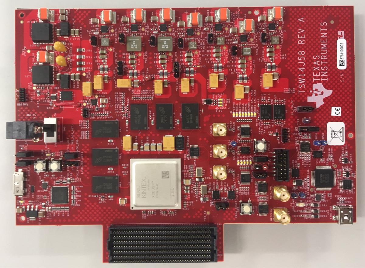
In pattern generator mode, the TSW14J58 generates the desired test patterns for DAC EVMs under test. These patterns are sent from the host PC over the USB interface to the TSW14J58. The FPGA stores the data received into the board DDR4 memory module. The data from memory is then read by the FPGA and transmitted to a DAC EVM across the FMC+ interface connector. The board contains a 200-MHz oscillator used to generate the DDR4 reference clock and a general purpose clock. shows the TI TSW14J58 evaluation module.
 Figure 2-1 TSW14J58EVM
The major features of the TSW14J58 are:
- Backward-compatible with JESD204B (Subclasses: 0 1, 2)
- Support for deterministic latency
- Serial lanes speeds up to 24.5 Gbps
- 16 routed transceiver channels
- 24Gb DDR4 SDRAM (split into two banks of 3 independent 256 × 16, 4Gb SDRAMs). Quarter rate DDR4 controllers supporting up to 1200-MHz operation
- 1.536G of 16-bit samples of onboard memory
- Supports 1.8-V CMOS IO standard for spare FMC+ signals
- General purpose 200-MHz oscillator
- Onboard FTDI FT601Q-B USB 3.0 device for parallel interface to the FPGA
- Onboard FTDI FT4232H USB 2.0 device for FPGA JTAG interface (downloading firmware) and general purpose I/O interface to onboard functions and FMC+
- Reference clocking for transceivers available through FMC+ port or SMAs
- Supported by TI HSDC PRO software
- FPGA firmware developed with Xilinx Vivado development tool.
- JESD RX IP core with support for:
- USB and JTAG reconfigurable JESD core parameters: L, M, K, F, HD, S, and more
- ILA configuration data accessible through USB and JTAG
- Lane alignment and character replacement enabled or disabled through USB and JTAG
- JESD TX IP core with support for:
- USB and JTAG reconfigurable JESD core parameters: L, M, K, F, HD, S, and more
- ILA configuration data accessible through USB and JTAG
- Dynamically reconfigurable Transceiver data rate.
- Serial lane operating range from 1 to 24.5 Gbps
- JESD RX IP core with support for:
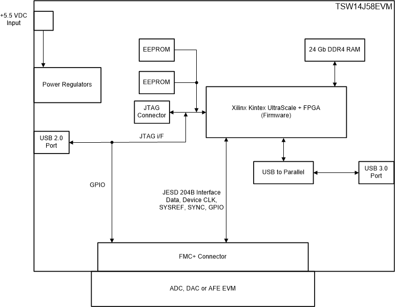
Figure 2-2 shows a block diagram of the TSW14J58 EVM.
 Figure 2-2 TSW14J58EVM Block Diagram