SNAU182A March   2021  – May 2022


  1.   Trademarks
  2. 1LMX2571EPEVM Evaluation Module
    1. 1.1 Evaluation Module Contents
    2. 1.2 Evaluation Setup Requirement
    3. 1.3 Resources
  3. 2Setup
    1. 2.1 Connection Diagram
    2. 2.2 Power Supply
    3. 2.3 Reference Clock
    4. 2.4 RF Output
    5. 2.5 Programming
    6. 2.6 Evaluation Software
    7. 2.7 EVM Strap Options
      1. 2.7.1 J11 Header
      2. 2.7.2 J12 Header
  4. 3Typical Measurement
    1. 3.1 Default Configuration
      1. 3.1.1 Loop Filter
      2. 3.1.2 Typical Output
    2. 3.2 Additional Tests
      1. 3.2.1 FSK Modulation
      2. 3.2.2 Register Readback
  5. 4Schematic
  6. 5Board Construction
    1. 5.1 PCB Layer Stack-Up
    2. 5.2 PCB Layout
  7. 6Bill of Materials
  8. 7Troubleshooting Guide
  9.   A Using Different Reference Clock
  10.   B Reference PRO
    1.     B.1 Output Frequency Selection
    2.     B.2 Output Format Selection
    3.     B.3 Typical Output Characteristics
    4.     B.4 Firmware Update
  11.   C Revision History

J12 Header

Pin 2 of J12 is connected to the CE pin. Put a short to the HW position, this will connect the CE pin to 3V3 through resistor R38. If the short is placed in the SW position, the status of CE pin is configurable through TICS Pro.
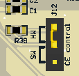
GUID-2EB79F28-E2BC-4BAC-AC64-6745B2AE0426-low.png Figure 2-5 J12 Header