SNLS493A October 2014 – January 2015 DS80PCI810
PRODUCTION DATA.
- 1 Features
- 2 Applications
- 3 Description
- 4 Revision History
- 5 Pin Configuration and Functions
- 6 Specifications
- 7 Detailed Description
- 8 Applications and Implementation
- 9 Power Supply Recommendations
- 10Layout
- 11Device and Documentation Support
- 12Mechanical, Packaging, and Orderable Information
8 Applications and Implementation
NOTE
Information in the following applications sections is not part of the TI component specification, and TI does not warrant its accuracy or completeness. TI’s customers are responsible for determining suitability of components for their purposes. Customers should validate and test their design implementation to confirm system functionality.
8.1 Application Information
8.1.1 DS80PCI810 versus DS80PCI800
The DS80PCI810 and DS80PCI800 are pin compatible, and both can be used for PCIe Gen-1, 2, and 3 applications. The DS80PCI810 features several design enhancements to improve PCIe system interoperability and performance over the previous generation DS80PCI800 design. The DS80PCI810 has a more linear input equalizer and output driver to enhance signal transparency for protocols requiring link training. This transparency is important, because it preserves subtle pre-cursor and post-cursor information from the Tx signal prior to the repeater. As a result of these enhancements, the DS80PCI810 is easier to tune and increases flexibility of IC placement along the signal path. The DS80PCI810 is ideal for open PCIe systems. An open system is defined as an environment where a PCIe connector accepts any compliant PCIe Add-In Card (AIC). The DS80PCI810 can extend the reach of a PCIe system by up to 10 dB beyond the max allowable PCIe channel loss.
The DS80PCI800 may still be used for closed PCIe systems where significant insertion losses (> 35 dB at 4 GHz) are expected in the signal path. In contrast to open PCIe systems, a closed system is defined as a PCIe environment with a limited number of possible Host-to-Endpoint combinations. Due to larger CTLE gain, the DS80PCI800 is able to compensate insertion loss over longer transmission lines before the repeater. In addition, the DS80PCI800 is able to produce de-emphasis levels up to -12 dB to support significant trace losses after the repeater (-15 dB at 4 GHz).
8.1.2 Signal Integrity in PCIe Applications
In PCIe Gen-3 applications, specifications require Rx-Tx link training to establish and optimize signal conditioning settings at 8 Gbps. In link training, the Rx partner requests a series of FIR coefficients from the Tx partner at speed. This training sequence is designed to pre-condition the signal path with an optimized link between the endpoints. Note that there is no link training with Tx FIR coefficients for PCIe Gen-1 (2.5 Gbps) or PCIe Gen-2 (5.0 Gbps) applications.
The DS80PCI810 works to extend the reach possible by using active linear equalization on the channel, boosting attenuated signals so that they can be more easily recovered at the Rx. The repeater outputs are specially designed to be transparent to Tx FIR signaling in order to pass information critical for optimal link training to the Rx. Suggested settings for the A-channels and B-channels are given in Table 10 and Table 11. Further adjustments to EQx and VODx settings may optimize signal margin on the link for different system applications:
Table 10. Suggested Device Settings in Pin Mode
| CHANNEL SETTINGS | PIN MODE |
|---|---|
| EQx | Level 4 |
| VODx[1:0] | Level 6 (1, 0) |
Table 11. Suggested Device Settings in SMBus Modes
| CHANNEL SETTINGS | SMBus MODES |
|---|---|
| EQx | 0x03 |
| VODx | 110'b |
| VOD_DB | 000'b |
The SMBus Slave Mode code example in Table 12 may be used to program the DS80PCI810 with the recommended device settings.
Table 12. SMBus Example Sequence
| REGISTER | WRITE VALUE | COMMENTS | ||
|---|---|---|---|---|
| 0x06 | 0x18 | Set SMBus Slave Mode Register Enable. | ||
| 0x0F | 0x03 | Set CHB_0 EQ to 0x03. | ||
| 0x10 | 0xAE | Set CHB_0 VOD to 110'b. | ||
| 0x11 | 0x00 | Set CHB_0 VOD_DB to 000'b. | ||
| 0x16 | 0x03 | Set CHB_1 EQ to 0x03. | ||
| 0x17 | 0xAE | Set CHB_1 VOD to 110'b. | ||
| 0x18 | 0x00 | Set CHB_1 VOD_DB to 000'b. | ||
| 0x1D | 0x03 | Set CHB_2 EQ to 0x03. | ||
| 0x1E | 0xAE | Set CHB_2 VOD to 110'b. | ||
| 0x1F | 0x00 | Set CHB_2 VOD_DB to 000'b. | ||
| 0x24 | 0x03 | Set CHB_3 EQ to 0x03. | ||
| 0x25 | 0xAE | Set CHB_3 VOD to 110'b. | ||
| 0x26 | 0x00 | Set CHB_3 VOD_DB to 000'b. | ||
| 0x2C | 0x03 | Set CHA_0 EQ to 0x03. | ||
| 0x2D | 0xAE | Set CHA_0 VOD to 110'b. | ||
| 0x2E | 0x00 | Set CHA_0 VOD_DB to 000'b. | ||
| 0x33 | 0x03 | Set CHA_1 EQ to 0x03. | ||
| 0x34 | 0xAE | Set CHA_1 VOD to 110'b. | ||
| 0x35 | 0x00 | Set CHA_1 VOD_DB to 000'b. | ||
| 0x3A | 0x03 | Set CHA_2 EQ to 0x03. | ||
| 0x3B | 0xAE | Set CHA_2 VOD to 110'b. | ||
| 0x3C | 0x00 | Set CHA_2 VOD_DB to 000'b. | ||
| 0x41 | 0x03 | Set CHA_3 EQ to 0x03. | ||
| 0x42 | 0xAE | Set CHA_3 VOD to 110'b. | ||
| 0x43 | 0x00 | Set CHA_3 VOD_DB to 000'b. | ||
8.1.3 Rx Detect Functionality in PCIe Applications
In PCIe systems, specifications require the Tx to implement Rx detection in order to determine whether an Rx endpoint is present. Since the DS80PCI810 is designed for placement between an ASIC Tx and endpoint Rx, the DS80PCI810 implements automatic polling for valid Rx detection when the RXDET pin is left floating or tied low via 20 kΩ to GND. If 50 Ω impedances are seen on both positive and negative outputs of a DS80PCI810 channel, the Rx detect state machine asserts Rx detection, and a 50 Ω termination to VDD is provided at the respective channel's positive and negative input. For open PCIe systems where users may swap multiple cards in and out of a given PCIe slot, it is recommended to keep the RXDET pin floating. For closed systems where an endpoint Rx is present in a PCIe slot at all times, the RXDET pin may be left floating or tied high via 1 kΩ to VDD (2.5 V mode) or VIN (3.3 V mode).
For more details about DS80PCI810 Rx detection, refer to Table 2.
8.2 Typical Applications
8.2.1 Generic High Speed Repeater
The DS80PCI810 extends PCB and cable reach in multiple applications by using active linear equalization. The high linearity of this device aids specifically in protocols requiring link training and can be used in line cards, backplanes, and motherboards, thereby improving margin and overall eye performance. The capability of the repeater can be explored across a range of data rates and ASIC-to-link-partner signaling, as shown in the following two test setup connections.
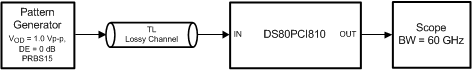 Figure 9. Test Setup Connections Diagram
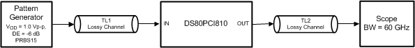 Figure 10. Test Setup Connections Diagram
8.2.1.1 Design Requirements
As with any high speed design, there are many factors that influence the overall performance. Below are a list of critical areas for consideration and study during design.
- Use 100 Ω impedance traces. Generally these are very loosely coupled to ease routing length differences.
- Place AC-coupling capacitors near to the receiver end of each channel segment to minimize reflections.
- The maximum body size for AC-coupling capacitors is 0402.
- Back-drill connector vias and signal vias to minimize stub length.
- Use reference plane vias to ensure a low inductance path for the return current.
8.2.1.2 Detailed Design Procedure
The DS80PCI810 is designed to be placed at an offset location with respect to the overall channel attenuation. In order to optimize performance, the repeater requires tuning to extend the reach of the cable or trace length while also recovering a solid eye opening. To tune the repeater, the settings mentioned in Table 10 (for Pin Mode) and Table 11 (for SMBus Modes) are recommended as a default starting point for most applications. Once these settings are configured, additional tuning of the EQ and, to a lesser extent, VOD may be required to optimize the repeater performance for each specific application environment.
Examples of the repeater performance as a generic high speed datapath repeater are illustrated in the performance curves in the next section.
8.2.1.3 Application Performance Plots
8.2.1.3.1 Pre-Channel Only Setup
TJ (1.0E-12) = 21.6 ps
No Repeater, 8 Gbps

TJ (1.0E-12) = 43.7 ps
No Repeater, 8 Gbps
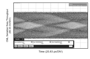
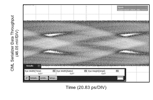
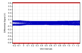
TJ (1.0E-12) = Not Available Due to Closed Eye
No Repeater, 8 Gbps
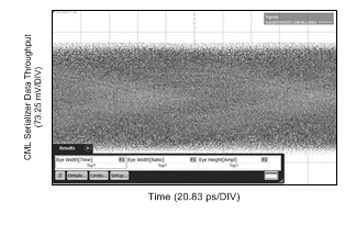
TJ (1.0E-12) = Not Available Due to Closed Eye
No Repeater, 8 Gbps
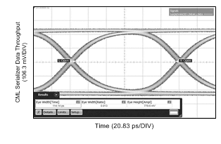
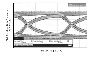
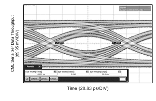
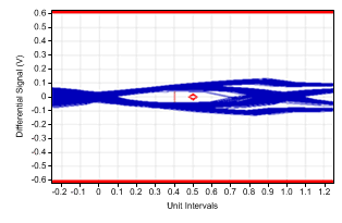
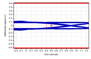
TJ (1.0E-12) = 13.6 ps
DS80PCI810 CHA_0, 8 Gbps
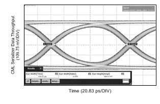
TJ (1.0E-12) = 18.1 ps
DS80PCI810 CHA_0, 8 Gbps
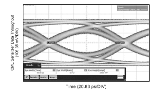
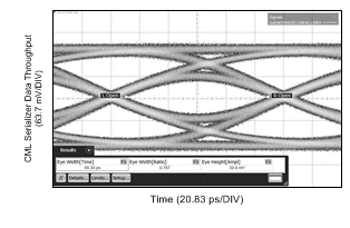
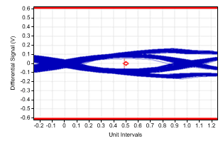
TJ (1.0E-12) = 35.5 ps
DS80PCI810 CHA_0, 8 Gbps
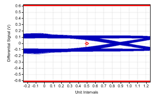
TJ (1.0E-12) = 41.4 ps
DS80PCI810 CHA_0, 8 Gbps
8.2.1.3.2 Pre-Channel and Post-Channel Setup
TJ (1.0E-12) = Not Available Due to Closed Eye
TL2 = 10 Inch 5–Mil FR4 Trace,
No Repeater, 8 Gbps
TJ (1.0E-12) = 33.0 ps
TL2 = 10 Inch 5–Mil FR4 Trace,
DS80PCI810 CHA_0, 8 Gbps
8.2.2 PCIe Board Applications (PCIe Gen-3)
The DS80PCI810 can be used to extend trace length on motherboards and line cards in PCIe Gen-3 applications. The high linearity of the DS80PCI810 aids in the link training protocol required by PCIe Gen-3 at 8 Gbps in accordance with PCI-SIG standards. For PCIe Gen-3, preservation of the pre-cursor and post-cursor Tx FIR presets (P0-P10) is crucial to successful signal transmission from motherboard system root complex to line card ASIC or Embedded Processor. Below is a typical example of the DS80PCI810 used in a PCIe application:
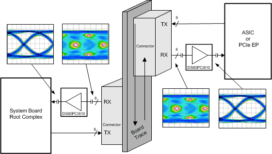 Figure 21. Typical PCIe Gen-3 Configuration Diagram
8.2.2.1 Design Requirements
As with any high speed design, there are many factors that influence the overall performance. Please reference Design Requirements in the Generic High Speed Repeater application section for a list of critical areas for consideration and study during design.
8.2.2.2 Design Procedure
In PCIe Gen-3 applications, there is a large range of flexibility regarding the placement of the DS80PCI810 in the signal path due to the high linearity of the device. If the PCIe slot must also support lower speeds like PCIe Gen-1 (2.5 Gbps) and Gen-2 (5.0 Gbps), it is recommended to place the DS80PCI810 closer to the endpoint Rx. Once the DS80PCI810 is placed on the signal path, the repeater must be tuned. To tune the repeater, the settings mentioned in Table 10 (for Pin Mode) and Table 11 (for SMBus Modes) are recommended as a default starting point for most applications. Once these settings are configured, additional tuning of the EQ and, to a lesser extent, VOD may be required to optimize the repeater performance to pass link training preset requirements for PCIe Gen-3.
An example of a test configuration used to evaluate the DS80PCI810 in this application can be seen in Figure 22. For more information about DS80PCI810 PCIe applications, please refer to application note SNLA227.
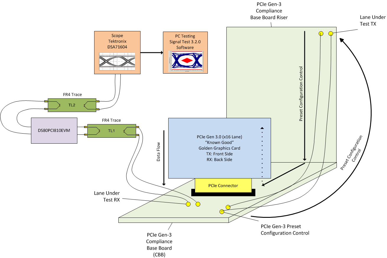 Figure 22. Typical PCIe Gen-3 Add-In Card Test Diagram
8.2.2.3 Application Performance Plots
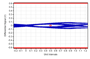
Composite Eye Height: 50.39 mV
Minimum Eye Width: 49.87 ps
Overall SigTest Result: Fail
TL1 = 10 Inch 4-Mil FR4 Trace, No TL2
No Repeater, 8 Gbps
Composite Eye Height: 50.39 mV
Minimum Eye Width: 49.87 ps
Overall SigTest Result: Fail
TL1 = 10 Inch 4-Mil FR4 Trace, No TL2
No Repeater, 8 Gbps
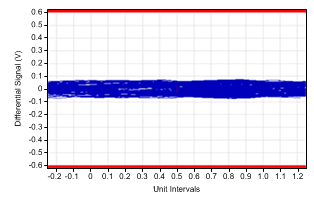
Composite Eye Height: 0.057 mV
Minimum Eye Width: 37.66 ps
Overall SigTest Result: Fail
TL1 = 10 Inch 4-Mil FR4 Trace,
TL2 = 5 Inch 4-Mil FR4 Trace
No Repeater, 8 Gbps
Composite Eye Height: 0.057 mV
Minimum Eye Width: 37.66 ps
Overall SigTest Result: Fail
TL1 = 10 Inch 4-Mil FR4 Trace,
TL2 = 5 Inch 4-Mil FR4 Trace
No Repeater, 8 Gbps
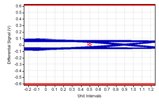
Composite Eye Height: 112.2 mV
Minimum Eye Width: 83.82 ps
Overall SigTest Result: Pass
TL1 = 10 Inch 4-Mil FR4 Trace, No TL2
DS80PCI810, 8 Gbps
Composite Eye Height: 112.2 mV
Minimum Eye Width: 83.82 ps
Overall SigTest Result: Pass
TL1 = 10 Inch 4-Mil FR4 Trace, No TL2
DS80PCI810, 8 Gbps
Composite Eye Height: 77.26 mV
Minimum Eye Width: 78.24 ps
Overall SigTest Result: Pass
TL1 = 10 Inch 4-Mil FR4 Trace,
TL2 = 5 Inch 4-Mil FR4 Trace
DS80PCI810, 8 Gbps
Composite Eye Height: 77.26 mV
Minimum Eye Width: 78.24 ps
Overall SigTest Result: Pass
TL1 = 10 Inch 4-Mil FR4 Trace,
TL2 = 5 Inch 4-Mil FR4 Trace
DS80PCI810, 8 Gbps