SNLU291B March 2021 – August 2022 MCT8316Z
4.6 Hardware Variant Settings
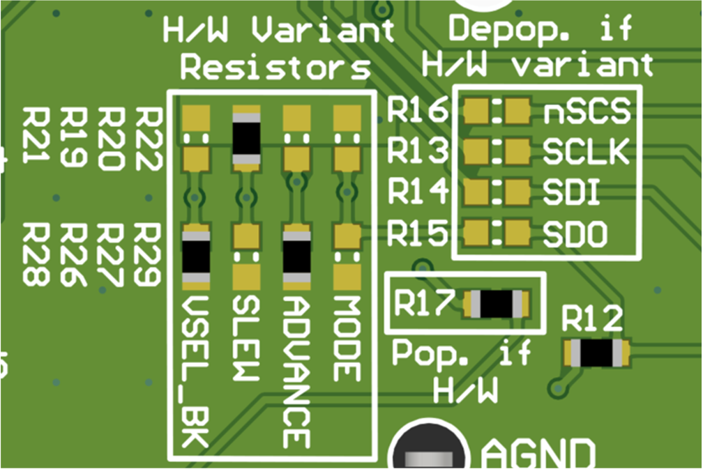
The MCT8316ZT device uses the configurable resistors to control the MODE, SLEW, ADVANCE, and VSEL_BUCK settings.
When using the MCT8316ZT, the SPI enable resistors in the “Depop. if H/W Variant” silk screen box are to be depopulated (R13–R16) and the resistor dividers in the “H/W Variant Resistors” silk screen box are populated with the desired settings (R19–R22 and R26–R29). This setup is shown in Figure 4-6.
 Figure 4-6 Resistor Divider Settings for MCT8316ZT (Hardware
Variant)
Figure 4-6 Resistor Divider Settings for MCT8316ZT (Hardware
Variant)Table 4-3 shows the user-adjustable resistor divider settings when using the MCT8316ZT. R19–R22 resistors connect to AVDD and R26–R29 resistors connect to AGND. The defaults of the two tables are in bold.
| Setting | Name | Description | Resistors (AVDD and AGND) |
Configuration | Setting |
|---|---|---|---|---|---|
| VSEL_BK | VBK | Buck regulator average voltage (LBK = 47 or 22 μH, |
R21 and R28 | R28 = 0 Ω | 3.3 V |
| R21 = R28 = DNP | 5.0 V | ||||
| R21 = 47 kΩ | 4.0 V | ||||
| R21 = 0 Ω | 5.7 V | ||||
| MODE | PWM Control Mode | Selects the Hall configuration, modulation, Asynchronous Rectification (ASR), and Automatic Asynchronous Rectification (AAR) settings | R22 and R29 | R29 = 0 Ω | Analog Hall Input, Asynchronous modulation, ASR and AAR Disabled |
| R29 = 22 kΩ | Digital Hall Input, Asynchronous modulation, ASR and AAR Disabled | ||||
| R29 = 100 kΩ | Analog Hall Input, Synchronous modulation, ASR and AAR Disabled | ||||
| R22 = R29 = DNP | Digital Hall Input, Synchronous modulation, ASR and AAR Disabled | ||||
| R22 = 100 kΩ | Analog Hall Input, Synchronous modulation, ASR and AAR Enabled | ||||
| R22 = 22 kΩ | Digital Hall Input, Synchronous modulation, ASR and AAR Enabled | ||||
| R22 = 0 Ω | Digital Hall Input, Asynchronous modulation, ASR and AAR Enabled | ||||
| SLEW | Slew Rate | Phase pin slew rate switching low to high (10-90%) and high to low (90-10%) | R19 and R26 | R26 = 0 Ω | 25 V/μs |
| R19 = R26 = DNP | 50 V/μs | ||||
| R19 = 47 kΩ | 125 V/μs | ||||
| R19 = 0 Ω | 200 V/μs | ||||
| ADV | Advance | Advances the lead angle by a selectable value (in electrical degrees) | R20 and R27 | R27 = 0 Ω | 0° |
| R27 = 22 kΩ | 4° | ||||
| R27 = 100 kΩ | 11° | ||||
| R20 = R27 = DNP | 15° | ||||
| R20 = 100 kΩ | 20° | ||||
| R20 = 22 kΩ | 25° | ||||
| R20 = 0 Ω | 30° |