SNOAA71 June 2021 LMP7704-SP , OPA4277-SP
Design Steps
- Calculate the
output voltage Vout for this circuit using the
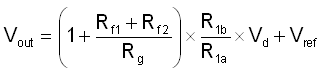
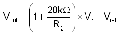
following equation:In this equation, Vd = V2 – V1 is the differential input voltage, Vref is set by R3 and R4 to level shift the output, and it is assumed that R1a = R2a and R1b = R2b. Integrated instrumentation amplifiers normally fix Rf1, Rf2, R1a, R2a, R1b, and R2b, leaving only Rg to set the gain of the circuit. In this discrete implementation, the designer has the freedom to alter all of these resistors, but the transfer function can be simplified by using standard values, such as Rf1 = Rf2 = R1a = R1b = R2a = R2b = 10kΩ, and using only Rg to set the gain. In this case, Rg can be calculated using the following simplified equation:
- Set
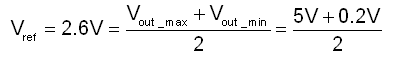
Vref. For this design, Vref
has been set as shown in the following equation so that a
symmetric input voltage range of –50mV to +50mV results in
an output voltage range of 0.2V to 5V.
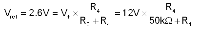 R4 = 13.83kΩ ≈ 13.8kΩ (standard value)Note: The magnitudes of R3 and R4 were chosen such that R3 || R4 is close to 10kΩ so that the low-pass filter formed by R3 || R4 and C2 is close to the common low-pass filter with R = 10kΩ and C = 100nF.
 - Choose
Rg to set the required gain using the
simplified transfer function.
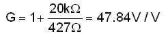
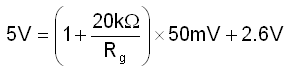 Rg = 425Ω ≈ 427Ω (standard value)This corresponds to a gain of: