SNOU195 july 2023 LDC5072-Q1
- 1
- Abstract
- Trademarks
- 1 Introduction
- 2 Gaining Access to the LDC5072 Sensor Design Tool
- 3 Installer Setup
- 4 Installing the Tool
- 5 Tool Overview
- 6 Using the Tool to Create a Design and Generate a Supporting SPICE Model and Gerber Files
- 7 Running Simulations in Pspice
- 8 Layout, Bill-of-Materials, and Schematic of the Test PC board
- 9 Troubleshooting
- 10Revision History
7 Running Simulations in Pspice
This section shows how the Spice models created by the tool can be used in a Spice transient simulation. These instructions assume the Spice models for the design have been created as described in the previous section.
All three models are usable in many Spice simulators, including Pspice for TI. The sensor and LDC5072 device models (SensorModel.cir, LDC5072.cir) can be imported and used as components in a larger schematic capture and/or circuit simulation, while the test bench file LDC5072_TB.cir can support a stand-alone Spice simulation. The remainder of this section gives an overview of how to use the test bench in a transient simulation using the Cadence Allegro Pspice Simulator.
The Cadence Allegro Pspice Simulator is started by selecting the PSpice AD application in the Windows Start menu as shown in the figure below. The number 17.4 refers to the version number of the tool used in this example.
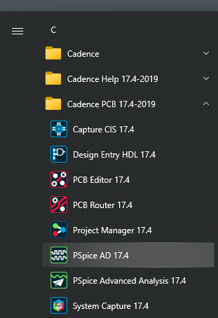 Figure 7-1 Starting the Cadence Allegro Pspice Simulator in the Windows Start Menu
The simulator window appears and resembles Figure 7-2.
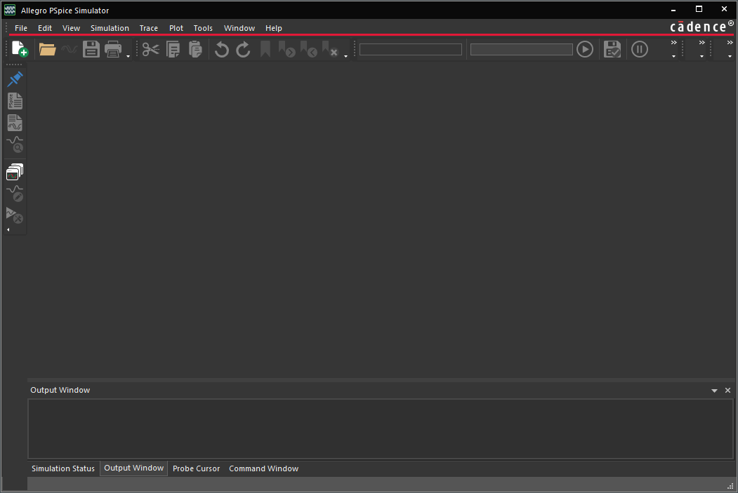 Figure 7-2 Cadence Allegro Pspice Simulator Window
As shown in Figure 7-3 and Figure 7-4, after the window appears the test bench is opened by selecting the File > Open command in the upper menu, and navigating to the application folder. The File Type field in the window needs to be changed to *.cir to be able to see the test bench file LDC5072_TB.cir. Select the file and click Open.
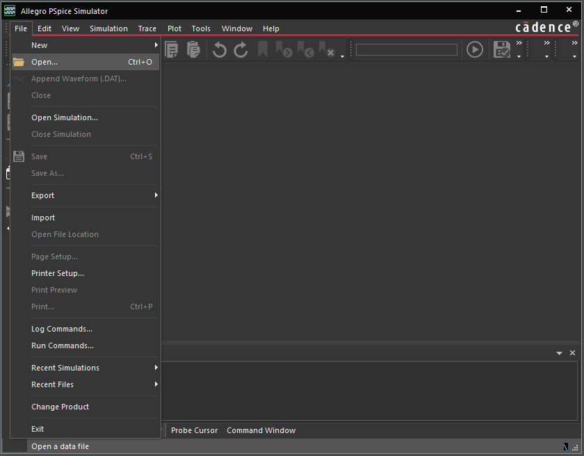 Figure 7-3 Opening the Spice Test Bench - Step 1
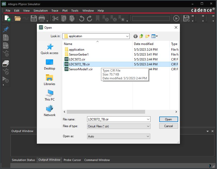 Figure 7-4 Opening the Spice Test Bench - Step 2
If you are using Pspice for TI you do not have the option of starting the Cadence Allegro Pspice Simulator directly from the Windows Start menu. You can easily access the simulator window by opening Pspice for TI and running a simulation of one of the built-in internal test benches. The Cadence Allegro Pspice Simulator window appears during or upon completion of the test bench simulation. After the completion of the simulation, close any plot windows and open your sensor design's test bench via the File > Open command in the upper menu and following the steps in the previous paragraph.
Opening the LDC5072_TB.cir file in Allegro can appear similar to the image shown just below. The upper parameters and comments reflect values for the sensor design. The first two .PARAM statements reflect the motor's rotational Max Velocity and Max Acceleration values chosen for this sensor design. For this example, the value in the comment "Target Electrical Rotation Rate in RPM = 1920000.0" results from the product of the parameters on the Mechanical Design tab Max Velocity (= 480 kRPM) and the Ratio Electrical to Mechanical (= 4). The .PARAM CLOAD = 10.000 n reflects the nominal load capacitance of the LDC5072 analog outputs. The parameters OSCSTARTUP, PERIOD, ACCPERIOD remain at their assigned values and do not change. The TEMP parameter was chosen in the Mechanical Design tab and reflects the modeled ambient temperature. The two .LIB statements include the sensor and LDC5072 device models in the test bench. Without those starements the test bench circuit is not complete.
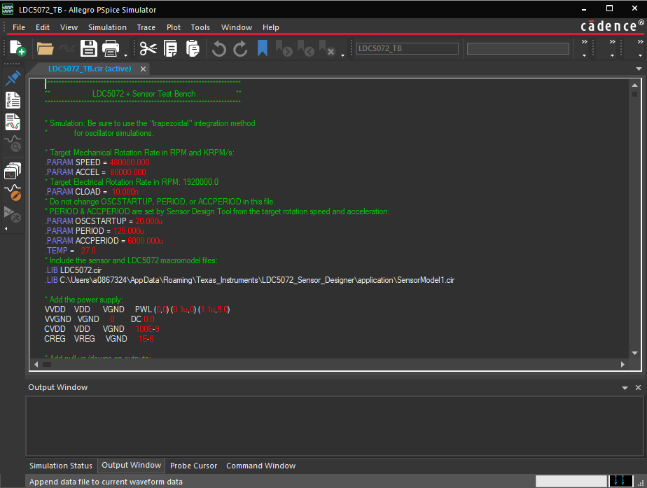 Figure 7-5 Sensor + LDC5072 Test Bench Open in Allegro Pspice Simulator
At the botton of the test bench file (see Figure 7-6) are the simulation analysis statements (.TRAN and .FOUR) and the uncommented .OPTIONS statements that set the convergence behavior (trade-off betwen simulation speed and accuracy) of the simulator. The .PROBE statements specify data-gathering for post-simulation plotting. Note that the last .PROBE statement has voltages that represent the mechanical angle, the computed electrical angle, and the ideal electrical angle (e.g. V(MECHANICAL), V(COMPUTED) and V(IDEAL)). The next-to-last .PROBE statement has differential voltages that represents the differential outputs of the LDC5072 output pins - V([XLDC5072.OUT01P],[XLDC5072.OUT01N]) and V([XLDC5072.OUT11P],[XLDC5072.OUT11N]).
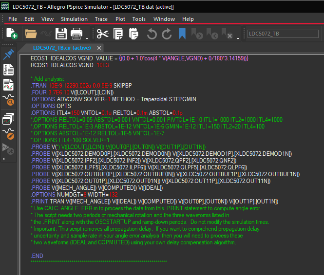 Figure 7-6 Test Bench Pspice Simulation Statements
The simulation is started by selecting Simulation > Run LDC5072_TB in the upper menu, or by clicking the right-pointing arrow in the upper banner as shown in the figures below. The simulation time depends on the design, the analysis parameters (.TRAN), and the .OPTIONS parameter values. If you are unfamiliar with Spice simulations, please be aware that some combinations of parameter values can result in long simulation times.
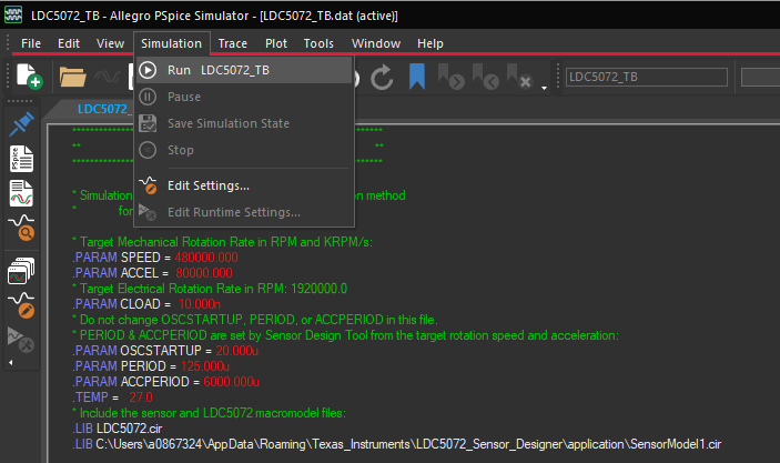 Figure 7-7 Starting the Pspice Test Bench Transient Simulation from the Simulation Menu
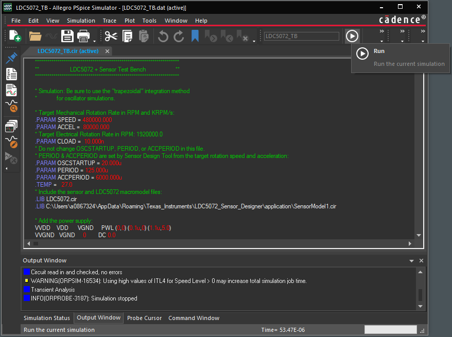 Figure 7-8 Starting the Pspice Test Bench Transient Simulation from the Run Button
While the simulation is running, you can see status messages in the Output Window, and the completion status as a percentage in the lower right-hand status bar.
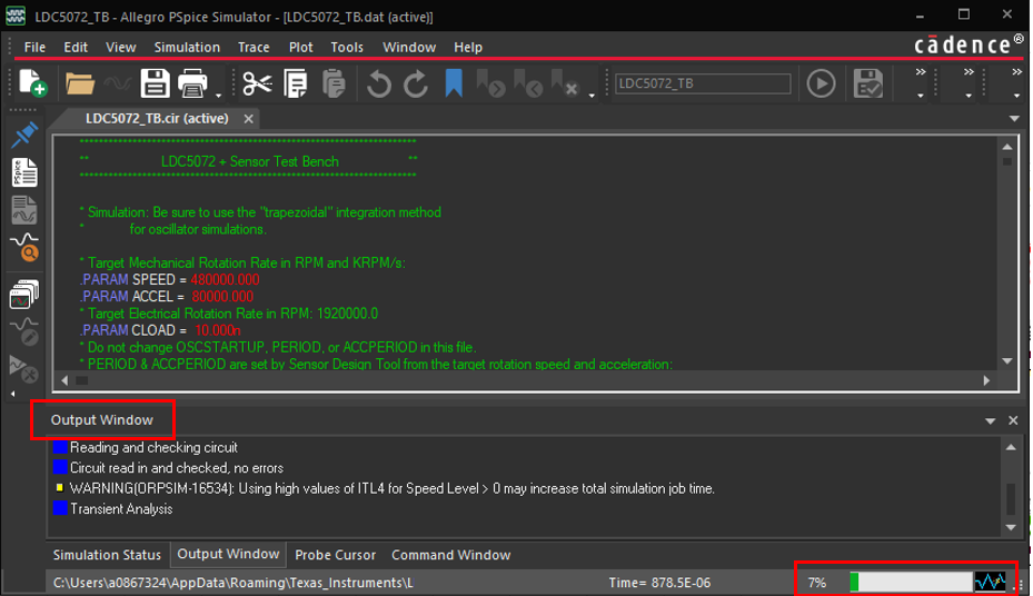 Figure 7-9 Status of a Running Pspice Simulation
For this example, the simulation is stopped after approximately 880 us, and the plot window appears as an additional tab in the simulator panel as shown in Figure 7-10. The next few steps illustrate how to plot the LD5072 output pins' voltages, as well as angle estimates that model the target angular rotation. You can plot the results by selecting either Trace/Add Trace, or by clicking the Add Trace button in the icon ribbon as shown in Figure 7-11.
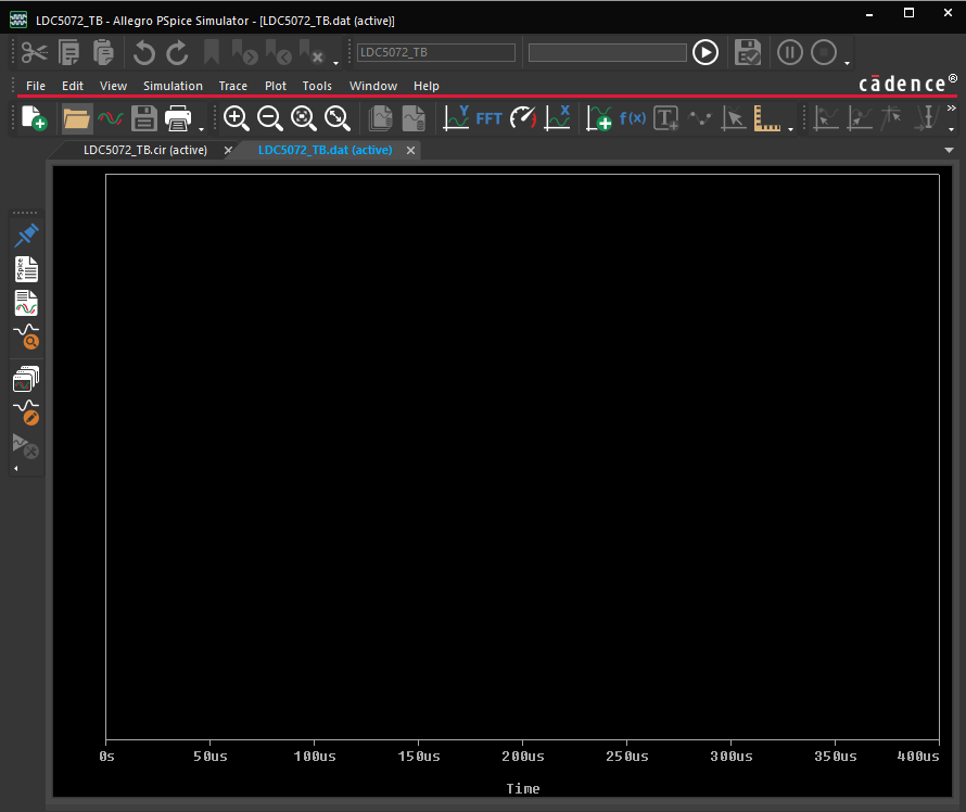 Figure 7-10 Initial Allegro Pspice Plot Window After Completion of Simulation
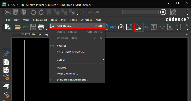 Figure 7-11 Adding a Trace to the Allegro Pspice Plot Window
The first step is to select the differential voltage of the LDC5072 channel 0 (COS) output pins and by first clicking Add Trace and selecting V(XLDC5072.OUT01P,XLDC5072.OUT01N) as shown in Figure 7-12.
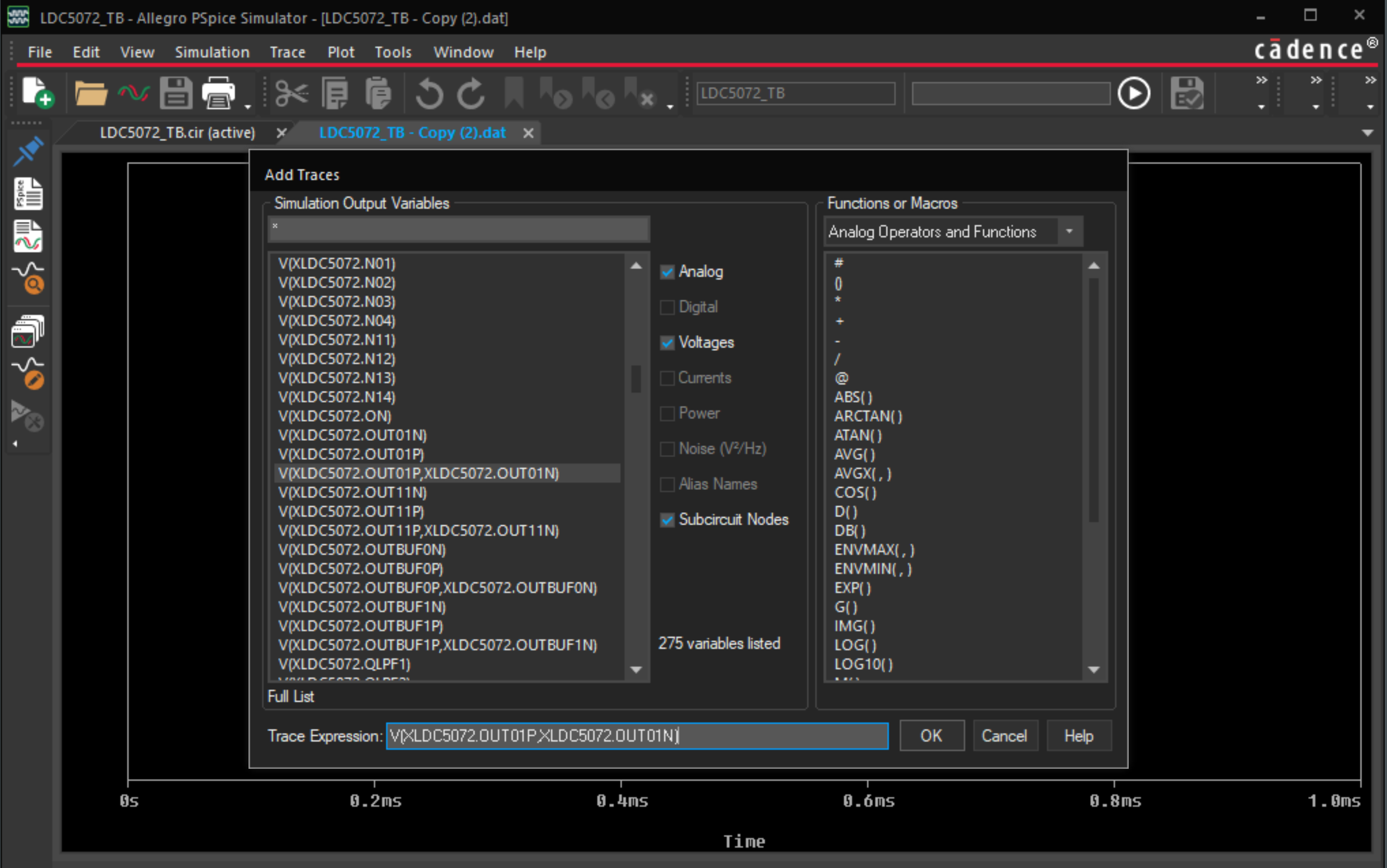 Figure 7-12 Adding the Trace for LDC5072 Channel 0 (COS) Differential Output Voltage
This shows a plot similar to Figure 7-13.
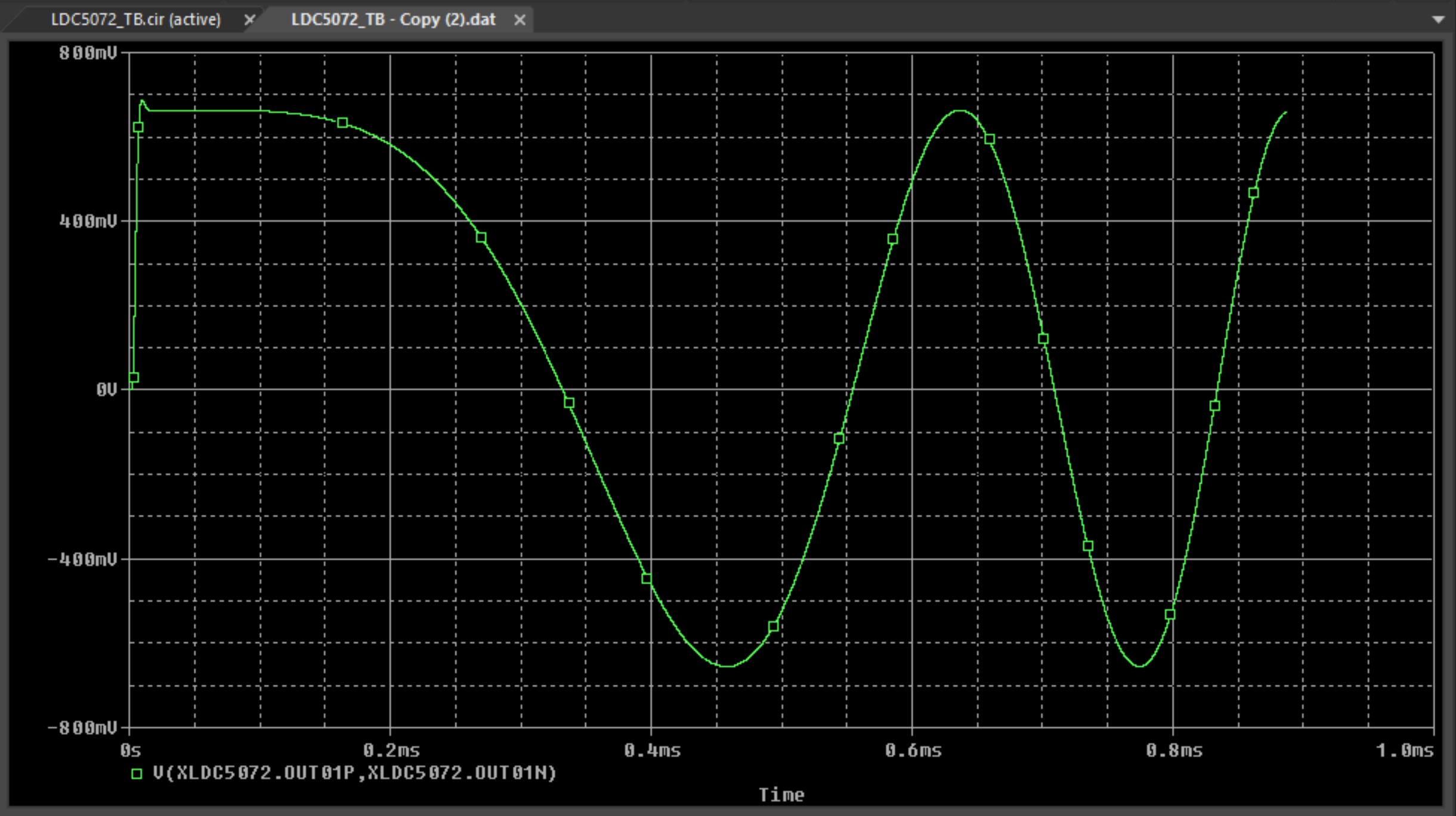 Figure 7-13 Plotted Curve for LDC5072 Channel 0 (COS) Differential Output Voltage
The second step is to add and select the differential voltage of the LDC5072 channel 1 (SIN) output pins by clicking Add Trace and selecting V(XLDC5072.OUT11P,XLDC5072.OUT11N).
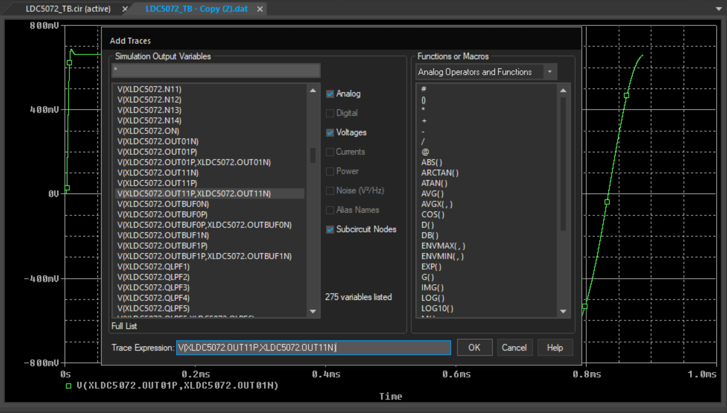 Figure 7-14 Adding the Trace for LDC5072 Channel 1 (SIN) Differential Output Voltage
This shows a plot similar to Figure 7-15.
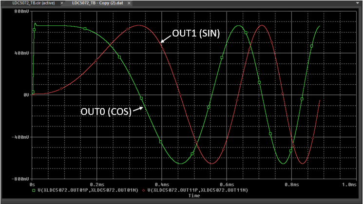 Figure 7-15 Plotted Curve for LDC5072 Channel 0 (COS) and Channel 1 (SIN) Differential Output Voltages
The next steps add an additional plot to the window to separate the LDC5072 pin voltage curves that were just plotted from the curves that show estimates of the target rotational angle. The first step is to add an additional plot window by selecting Plot/Add Plot to Window from the menu.
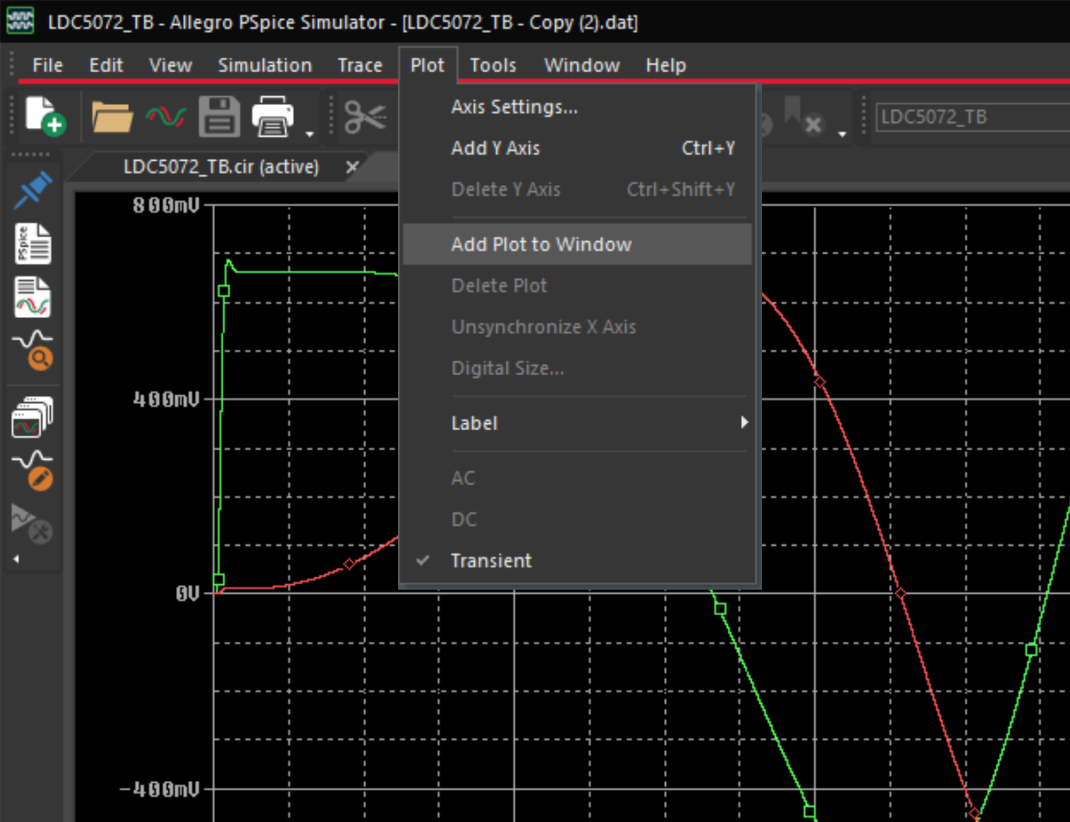 Figure 7-16 Adding a Plot Window
This places a new, empty plotting grid in the upper half of the plotting window.
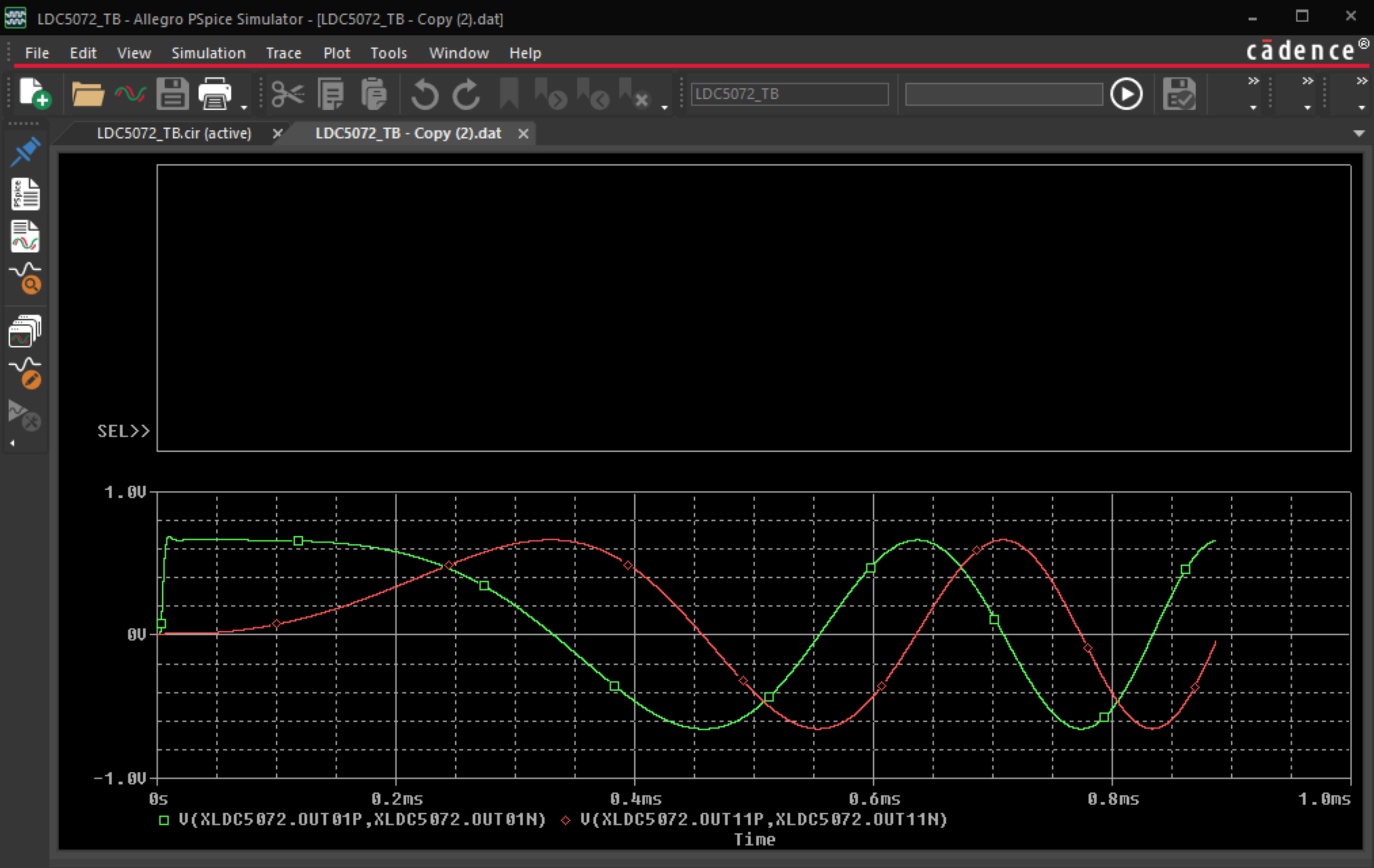 Figure 7-17 New Empty Plotting Window
Next add and plot the waveform that represents the physical angle of the target, which is represented by the the curve V(MECH_ANGLE) as shown in Figure 7-18 and Figure 7-19.
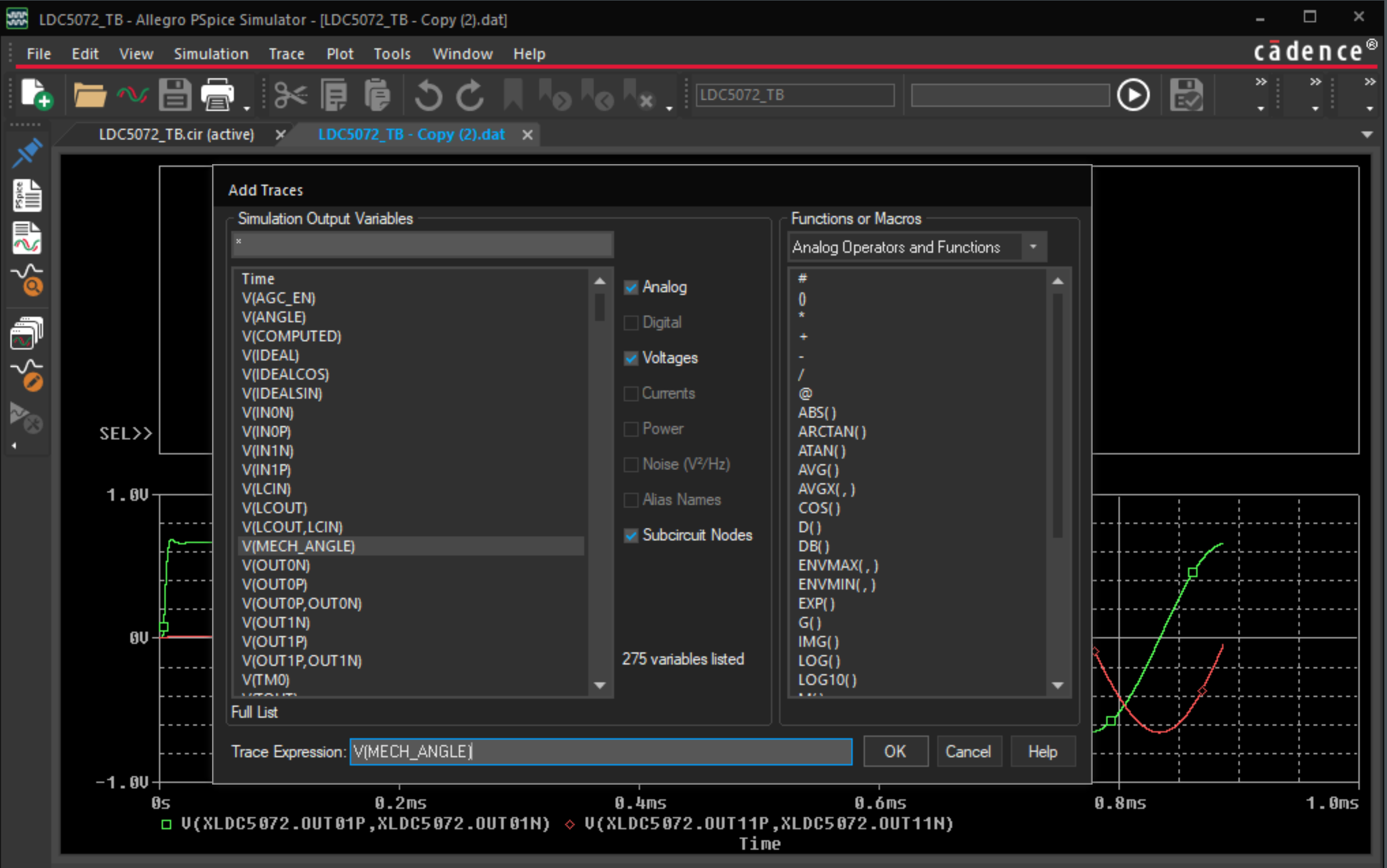 Figure 7-18 Add the Trace for the Target/Mechanical Angle
The plotted mechanical angle has an inital value of zero at the start of the simulation, but then moves between -180 degrees to 180 degrees as the target moves through full mechanical rotations. This is shown in Figure 7-19 where the units are displayed in volts, and represent the target position in degrees where one volt represents one degree of target rotation.
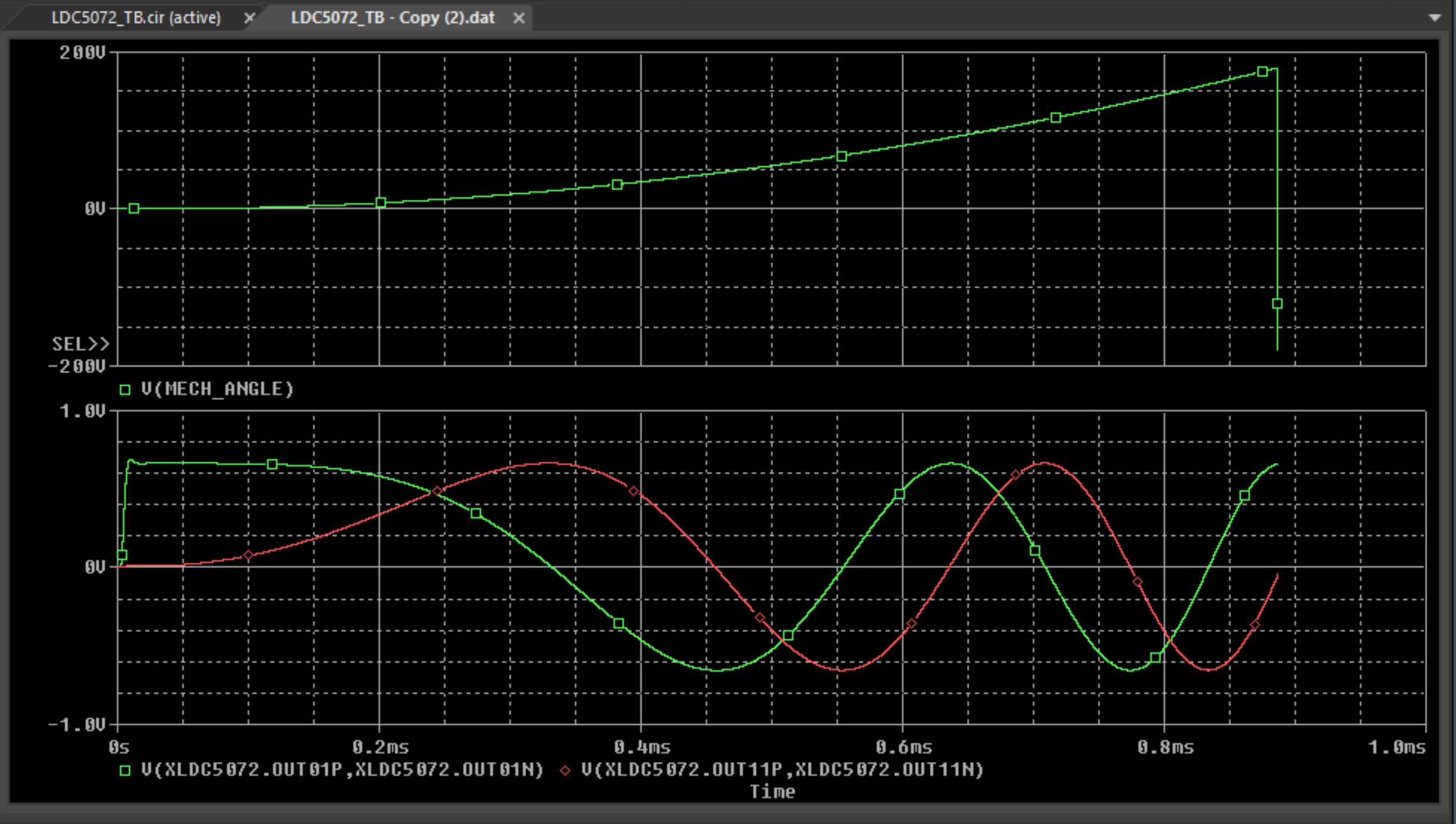 Figure 7-19 Addition of the Plotted Target/Mechanical Angle
Using similar steps, additional traces can be added which represent the computed electrical angle (V(COMPUTED)) and the angle (V(IDEAL)). The angle (V(COMPUTED)) is equal to the arctangent of the COS and SIN output channels and includes the effects of the time delays. The ideal electrical angle (V(IDEAL)) is also computed as an arctangent, but is based on the actual angle of the target and does not consider channel delays.
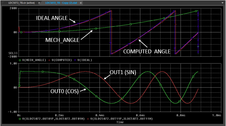 Figure 7-20 Add Waveforms of Computed and Ideal Electrical Angle
Fixed Gain Control
The gain of the LDC5072 Spice model can be changed by adjusting the values of RAGC1 and RAGC2 in the test bench file LDC5072_TB.cir. In the circuit file, the two resistors form a potentiometer with one end connected to VREG, and the other connected to GND and the mid-point (wiper) is connected to the AGC_EN pin of the device model (in file LDC5072.cir). The lines from the test bench netlist are shown just below.
* Bias for AGC_EN pin:
- RAGC1 VREG AGC_EN 7.0E3
- RAGC2 AGC_EN VGND 93.0E3
* Instantiate the sensor and LDC5072:
- XSENSOR LCIN LCOUT IN0P IN0N IN1P IN1N ANGLE VGND SensorModel
- XLDC5072 LCIN LCOUT IN0P IN0N IN1P IN1N OUT0P OUT0N OUT1P OUT1N VDD VREG VGND AGC_EN TM0 TOUT LDC5072
- + PARAMS: LPFI = 0.000 LPFQ = 0.000 DLYI = 0.190 DLYQ = 0.190 COUTLOAD = {CLOAD} ILIM = 3.000 m
- + IOFFSET = 0.000 QOFFSET = 0.000 IIMBAL = 0.000 QIMBAL = 0.000 INL = 0.01000
The values of RAGC1 and RAGC2 can be calculated via equation (7) in the device data sheet.
Where:
- Gain is the effective gain set by the gain block.
- %VREG is the voltage on the AGC_EN pin expressed as a percentage of the voltage on the VREG pin: Equation 2..