SNVA955A January 2020 – September 2020 LMQ61460 , LMQ61460-Q1 , LMQ62440-Q1
4 Pin Failure Mode Analysis (Pin FMA)
This section provides a Failure Mode Analysis (FMA) for the pins of the LMQ61460, LMQ61460-Q1, and LMQ62440-Q1. The failure modes covered in this document include the typical pin-by-pin failure scenarios:
- Pin short-circuited to Ground (see Table 4-2)
- Pin open-circuited (see Table 4-3)
- Pin short-circuited to an adjacent pin for LMQ61460 and LMQ61460-Q1 (see Table 4-4)
- Pin short-circuited to an adjacent pin for LMQ62440-Q1 (see Table 4-5)
- Pin short-circuited to supply (see Table 4-6)
Table 4-2 through Table 4-6 also indicate how these pin conditions can affect the device as per the failure effects classification in Table 4-1.
| Class | Failure Effects |
|---|---|
| A | Potential device damage that affects functionality |
| B | No device damage, but loss of functionality |
| C | No device damage, but performance degradation |
| D | No device damage, no impact to functionality or performance |
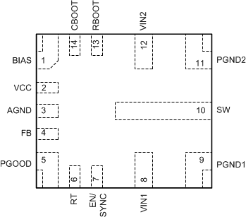
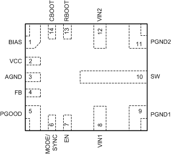
Figure 4-1 shows the LMQ61460, LMQ61460-Q1, and LMQ62440-Q1 pin diagram. For a detailed description of the device pins please refer to the 'Pin Configuration and Functions' section in the LMQ61460, LMQ61460-Q1, and LMQ62440-Q1 data sheet.
 Figure 4-1 Pin Diagram: LMQ61460, LMQ61460-Q1
 Figure 4-2 Pin Diagram: LMQ62440-Q1
- Application circuit, as per the LMQ61460-Q1 data sheet is used for LMQ61460 and LMQ61460-Q1.
- Application circuit, as per the LMQ62440-Q1 data sheet is used for the LMQ62440-Q1.
| Pin Name | Pin No | Description of Potential Failure Effect(s) | Failure Effect Class |
|---|---|---|---|
| BIAS | 1 | Normal Operation | D |
| VCC | 2 | VOUT=0V | B |
| AGND | 3 | Normal Operation | D |
| FB | 4 | VOUT >> than programmed output voltage. | B |
| PGOOD | 5 | PGOOD not valid signal. VOUT in regulation | D |
| RT | 6 | VOUT=0V | B |
|
MODE/SYNC |
Normal operation. Sets Auto mode |
D | |
| EN/SYNC | 7 | VOUT=0V | B |
|
EN |
VOUT=0V |
B | |
| VIN1 | 8 | VOUT=0V | B |
| PGND1 | 9 | VOUT normal | D |
| SW | 10 | Damage to HS FET | A |
| PGND2 | 11 | VOUT normal | D |
| VIN2 | 12 | VOUT=0V | B |
| RBOOT | 13 | VOUT=0V | A |
| CBOOT | 14 | VOUT=0V | B |
| Pin Name | Pin No | Description of Potential Failure Effect(s) | Failure Effect Class |
|---|---|---|---|
| BIAS | 1 | Normal Operation | D |
| VCC | 2 | VCC output will be unstable and can increase above 5.5V rating of VCC pin | A |
| AGND | 3 | VOUT might be abnormal due to switching noise on analog circuits | B |
| FB | 4 | VOUT >> than programmed output voltage. | B |
| PGOOD | 5 | PGOOD not valid signal. VOUT in regulation | D |
| RT | 6 | VOUT=0V | B |
|
MODE/SYNC |
Mode may switch randomly. Unpredictable behavior |
C | |
| EN/SYNC | 7 | VOUT=0V | B |
|
EN |
Device may shut off |
B | |
| VIN1 | 8 | VOUT normal. Current loop will be affected, potentially affecting noise/jitter/EMI/reliability. | C |
| PGND1 | 9 | VOUT normal. Current loop will be affected, potentially affecting noise/jitter/EMI/reliability. | C |
| SW | 10 | VOUT=0V | B |
| PGND2 | 11 | VOUT normal. All current will be in this loop, potentially affecting noise/jitter/EMI/reliability. | C |
| VIN2 | 12 | VOUT normal. All current will be in this loop, potentially affecting noise/jitter/EMI/reliability. | C |
| RBOOT | 13 | VOUT normal | D |
| CBOOT | 14 | VOUT=0V | B |
| Pin Name | Pin No | Description of Potential Failure Effect(s) | Failure Effect Class |
|---|---|---|---|
| BIAS | 1 | VCC ESD clamp damaged if BIAS > 5V. | A |
| VCC | 2 | VOUT=0V | B |
| AGND | 3 | VOUT >> than programmed output voltage. | B |
| FB | 4 | VOUT=0V, Damage if PGOOD>16V | A |
| PGOOD | 5 | VOUT=0V | B |
| RT | 6 | VOUT=0V, Damage if EN/SYNC>5.5V | A |
| EN/SYNC | 7 | VOUT normal | D |
| VIN1 | 8 | VOUT=0V | B |
| PGND1 | 9 | VOUT=0V. Damage to low-side circuitry if PGND >> AGND | B |
| SW | 10 | Damage to HS FET | A |
| PGND2 | 11 | VOUT=0V. Damage to low-side circuitry if PGND >> AGND | B |
| VIN2 | 12 | VOUT=0V | B |
| RBOOT | 13 | VOUT normal | D |
| CBOOT | 14 | VOUT=0V | B |
| Pin Name | Pin No | Description of Potential Failure Effect(s) | Failure Effect Class |
|---|---|---|---|
| BIAS | 1 | VCC ESD clamp damaged if BIAS > 5V. | A |
| VCC | 2 | VOUT=0V | B |
| AGND | 3 | VOUT >> than programmed output voltage. | B |
| FB | 4 | VOUT=0V, Damage if PGOOD>16V | A |
| PGOOD | 5 | VOUT=0V | B |
|
MODE/SYNC | 6 | Mode may change, Damage if MODE/SYNC>5.5V | A |
| EN | 7 | Normal operation | D |
| VIN1 | 8 | VOUT=0V | B |
| PGND1 | 9 | VOUT=0V. Damage to low-side circuitry if PGND >> AGND | B |
| SW | 10 | Damage to HS FET | A |
| PGND2 | 11 | VOUT=0V. Damage to low-side circuitry if PGND >> AGND | B |
| VIN2 | 12 | VOUT=0V | B |
| RBOOT | 13 | VOUT normal | D |
| CBOOT | 14 | VOUT=0V | B |
| Pin Name | Pin No | Description of Potential Failure Effect(s) | Failure Effect Class |
|---|---|---|---|
| BIAS | 1 | If VIN exceeds 16V damage will occur. If below, normal operation | A |
| VCC | 2 | If VIN exceeds 5.5V damage will occur. | A |
| AGND | 3 | VOUT=0V. Damage to other pins referred to GND. | A |
| FB | 4 | If VIN exceeds 16V damage will occur. VOUT=0V. | A |
| PGOOD | 5 | VOUT=0V. PGOOD ESD clamp will run current to destruction | A |
| RT | 6 | VOUT=0V | B |
| MODE/SYNC | Damage if MODE/SYNC>5.5V |
A | |
| EN/SYNC | 7 | Normal Operation | D |
|
EN |
Normal Operation |
D | |
| VIN1 | 8 | Normal Operation | D |
| PGND1 | 9 | VOUT=0V. Damage to low-side circuitry if PGND >> AGND | B |
| SW | 10 | Damage to LS FET | A |
| PGND2 | 11 | VOUT=0V. Damage to low-side circuitry if PGND >> AGND | B |
| VIN2 | 12 | Normal Operation | D |
| RBOOT | 13 | VOUT=0V. RBOOT ESD clamp will run current to destruction. | A |
| CBOOT | 14 | VOUT=0V. CBOOT ESD clamp will run current to destruction. | A |