SNVAA93 December 2023 LM65645-Q1 , LM70660 , LM706A0 , LM706A0-Q1 , LM70840 , LM70840-Q1 , LM70860 , LM70860-Q1 , LM70880 , LM70880-Q1 , LMR38020-Q1 , LMR38025-Q1
2.2 CM Noise Emission Model
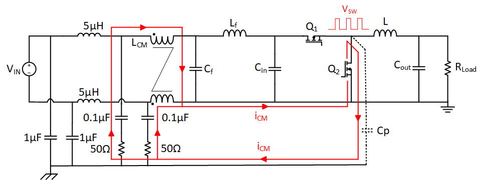
In addition to high di/dt causing DM-noise current, the high dv/dt at the SW node can also couple displacement current to ground through parasitic capacitance Cp. This coupled noise current is then returned by the power line and GND line in the same direction, resulting in CM noise.
Figure 2-5 illustrates the propagation path of CM noise. It can be observed that EMI filters (Lf and Cf) do not effectively hinder the propagation of CM noise, except when a common-mode choke (LCM) is added at the input wire. However, this solution can increase the system cost and solution size, and may not be feasible in some applications.
 Figure 2-5 Propagation Path of CM
Noise
Figure 2-5 Propagation Path of CM
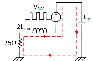
NoiseCM noise is influenced by dv/dt and Cp. It can be represented as a voltage source-driven model, as shown in Figure 3-22. The noise source can be reduced by either slowing down the dv/dt slew rate by adding a series Rboot with Cboot, or by reducing Cp by minimizing the SW node area.
 Figure 2-6 Emission Model of CM
Noise