SNVU543A November 2016 – December 2016 LM5170 , LM5170-Q1
-
LM5170-Q1 EVM User Guide
- Trademarks
- 1 Features and Electrical Performance
- 2 Setup
- 3 Test Procedure
- 4
Test Data
- 4.1 Efficiency
- 4.2 Current Regulation and Monitoring
- 4.3 Typical Master Enable Power Up and Shutdown
- 4.4 Channel Enable and Disable
- 4.5 Dual-Channel Interleaving Operation
- 4.6 ISETA Tracking
- 4.7 Diode Emulation Preventing Negative Currents
- 4.8 Dynamic DIR Change
- 4.9 Step Load Response
- 4.10 OVP
- 4.11 Output Short Circuit
- 5 Design Files
- Revision History
5.1 Schematics
To download the Schematics for the EVM board, see the design files at www.ti.com/tool.
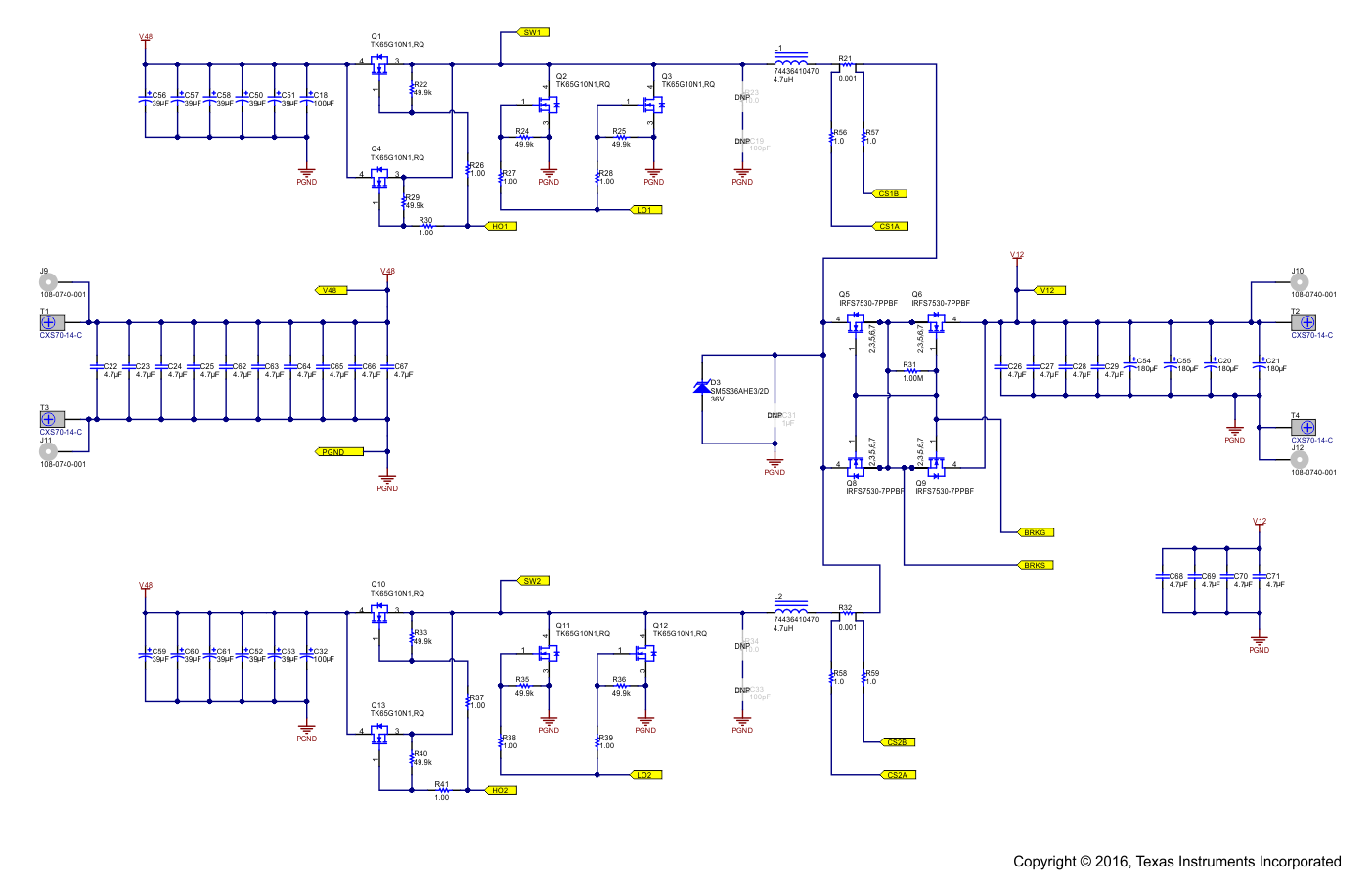 Figure 27. EVM Schematic Part 1: Power Circuit
 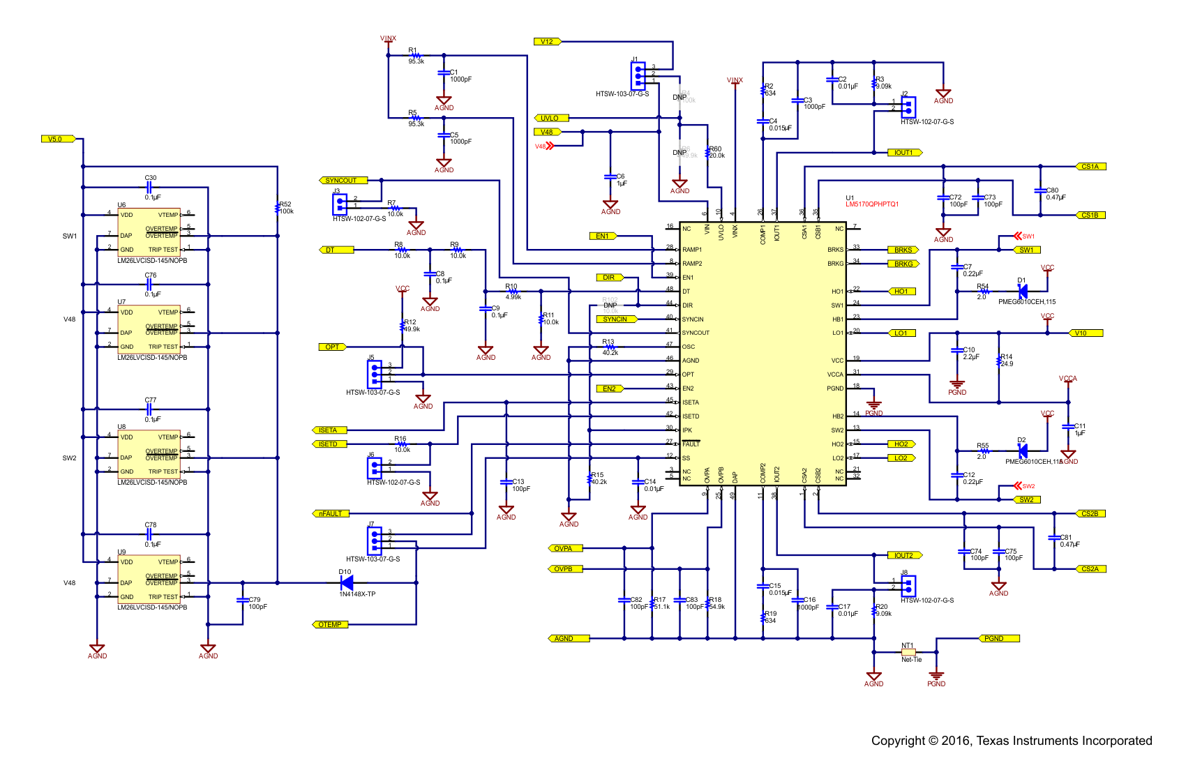 Figure 28. EVM Schematic Part 2: Control Circuit
 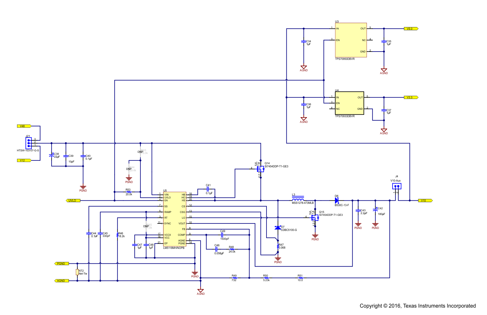 Figure 29. EVM Schematic Part 3: Bias Supplies
 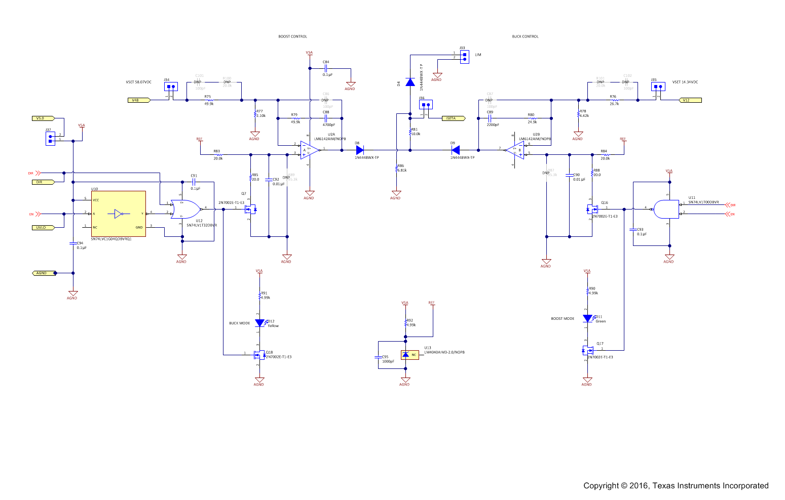 Figure 30. EVM Schematic Part 4: Optional Outer Voltage Loop Control Circuit
 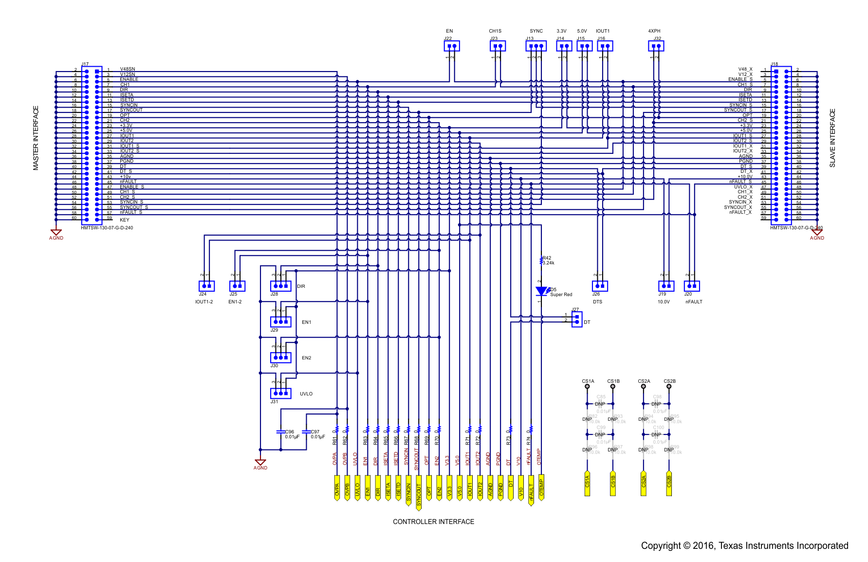 Figure 31. EVM Schematic Part 5: Interface Connectors and Configuration Headers