SNVU699 October 2020
4 Layout and Component Placement
Figure 4 and Figure 5 show the top and bottom assemblies of the printed circuit board (PCB) to show the component placement on the EVM.
Figure 6 and Figure 7 show the top and bottom layouts, Figure 8 and Figure 9 show the top and bottom layers, and Figure 10 shows the top solder mask of the EVM.
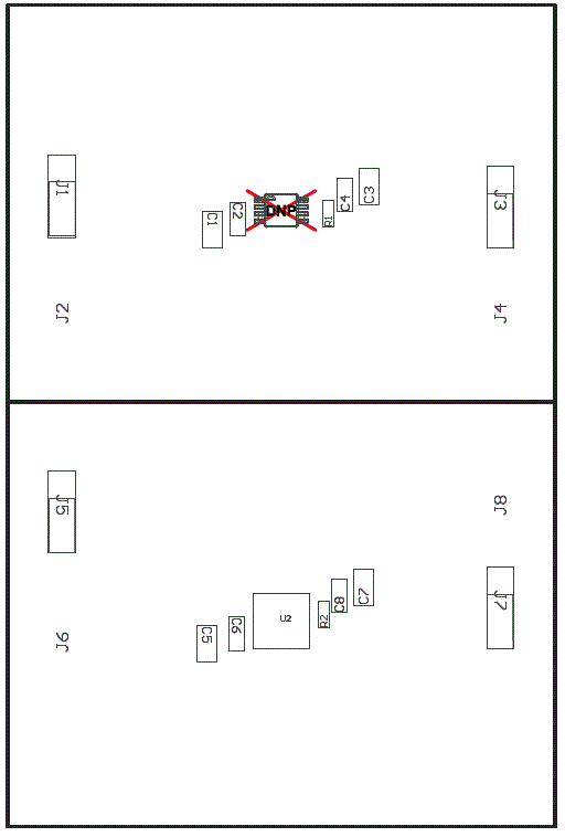 Figure 4-1 Component Placement—Top Assembly
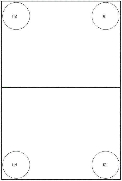 Figure 4-2 Component Placement—Bottom Assembly
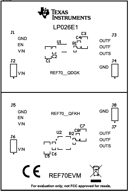 Figure 4-3 Layout Top
 Figure 4-4 Layout Bottom
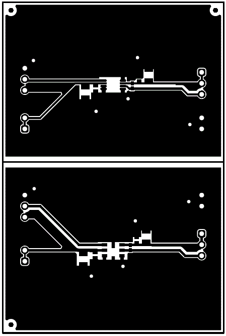 Figure 4-5 Top Layer
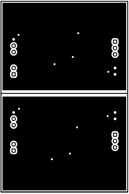 Figure 4-6 Bottom Layer
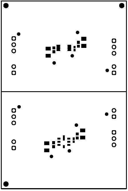 Figure 4-7 Top Solder Mask