SNVU745A January   2021  – May 2021 TPS62901 , TPS62902 , TPS62903


  1.   Trademarks
  2. 1Introduction
    1. 1.1 Performance Specification
    2. 1.2 Modifications
      1. 1.2.1 Input and Output Capacitors
      2. 1.2.2 Configurable Enable Threshold Voltage
      3. 1.2.3 SS/TR Capacitor
      4. 1.2.4 Feedforward Capacitor
      5. 1.2.5 MODE/S-CONF Resistor
      6. 1.2.6 Loop Response Measurement
  3. 2Setup
    1. 2.1 Input/Output Connector Descriptions
  4. 3Safety Instructions
  5. 4 Test Results
  6. 5 Board Layout
  7. 6Schematic and Bill of Materials
    1. 6.1 Schematic
    2. 6.2 Bill of Materials
  8. 7Revision History

Board Layout

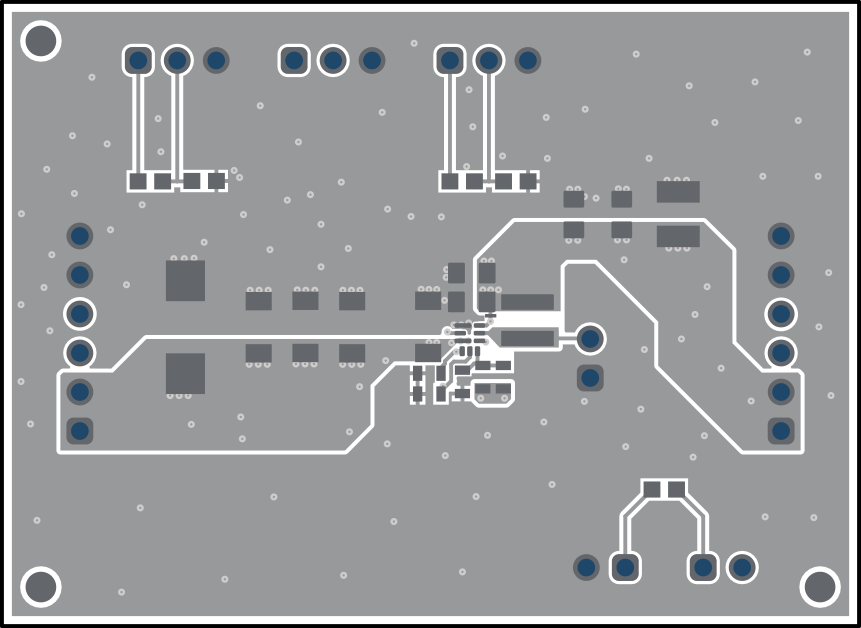
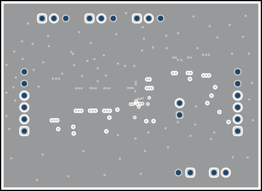
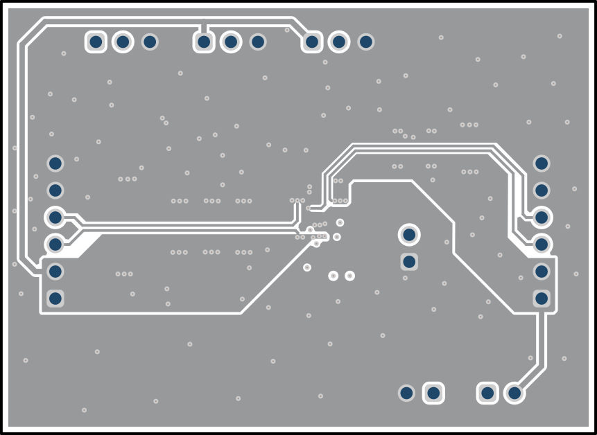
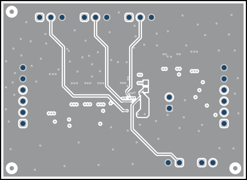
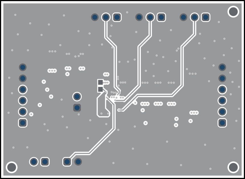
This section provides the EVM board layout and illustrations in Figure 5-1 through Figure 5-6. The Gerbers are available on the EVM product page.
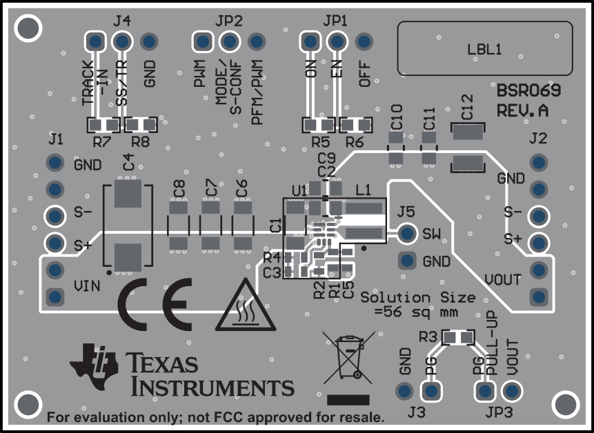
GUID-20210106-CA0I-GXSK-PX8S-HPJTC57JRB1X-low.gif Figure 5-1 Top Assembly
GUID-20210106-CA0I-VNDZ-N0LZ-Z4RQVQQXRJ6M-low.gif Figure 5-2 Top Layer
GUID-20210106-CA0I-FP8F-F0WT-9PGMRDXWTD7R-low.gif Figure 5-3 Internal Layer 1
GUID-20210106-CA0I-9ZRJ-HZLF-BMX3X78WBC3C-low.gif Figure 5-4 Internal Layer 2
GUID-20210106-CA0I-SG2B-HSDC-HPP15CDPJFFF-low.gif Figure 5-5 Bottom Layer
GUID-20210106-CA0I-LFNX-QVBG-BXTJ6H2G4RXN-low.gif Figure 5-6 Bottom Layer (Mirrored)