SPNA249 june 2023 TMS570LC4357-SEP
2 SEE Mechanisms
The primary single-event effect (SEE) event of interest in the TMS570LC4357-SEP is the destructive single-event latch-up (SEL). From a risk/impact point of view, the occurrence of an SEL is potentially the most destructive SEE event, and the biggest concern for space applications. The 12F021 (CMOS) process node was used for the TMS570LC4357-SEP. CMOS circuitry introduces a potential for SEL susceptibility. SEL can occur if excess current injection caused by the passage of an energetic ion is high enough to trigger the formation of a parasitic cross-coupled PNP and NPN bipolar structure (formed between the p-sub and n-well and N+ and P+ contacts). The parasitic bipolar structure initiated by a single-event creates a high-conductance path (inducing a steady-state current that is typically orders-of-magnitude higher than the normal operating current) between the power and ground that persists (is “latched”) until power is removed, or until the device is destroyed by the high-current state. The process modifications applied for the SEL-mitigation were sufficient, as the TMS570LC4357-SEP exhibited no SEL with heavy-ions up to an LETeff of 48 MeV-cm2/mg at a fluence of 1 x 10⁷ ions/cm2 and a chip temperature of 125°C.
This study was performed to evaluate the SEL effects with a bias voltage of VCCAD = 5.25 V; VCCIO = 3.6 V; VCC(core) = 1.32 V supply voltages. Heavy (47Ag) ions with LETeff of 48 MeV-cm2/mg were used to irradiate the devices. Flux of 105 ions/s-cm2 and fluence of 107 ions/cm2 were used during the exposure at 125°C temperature.
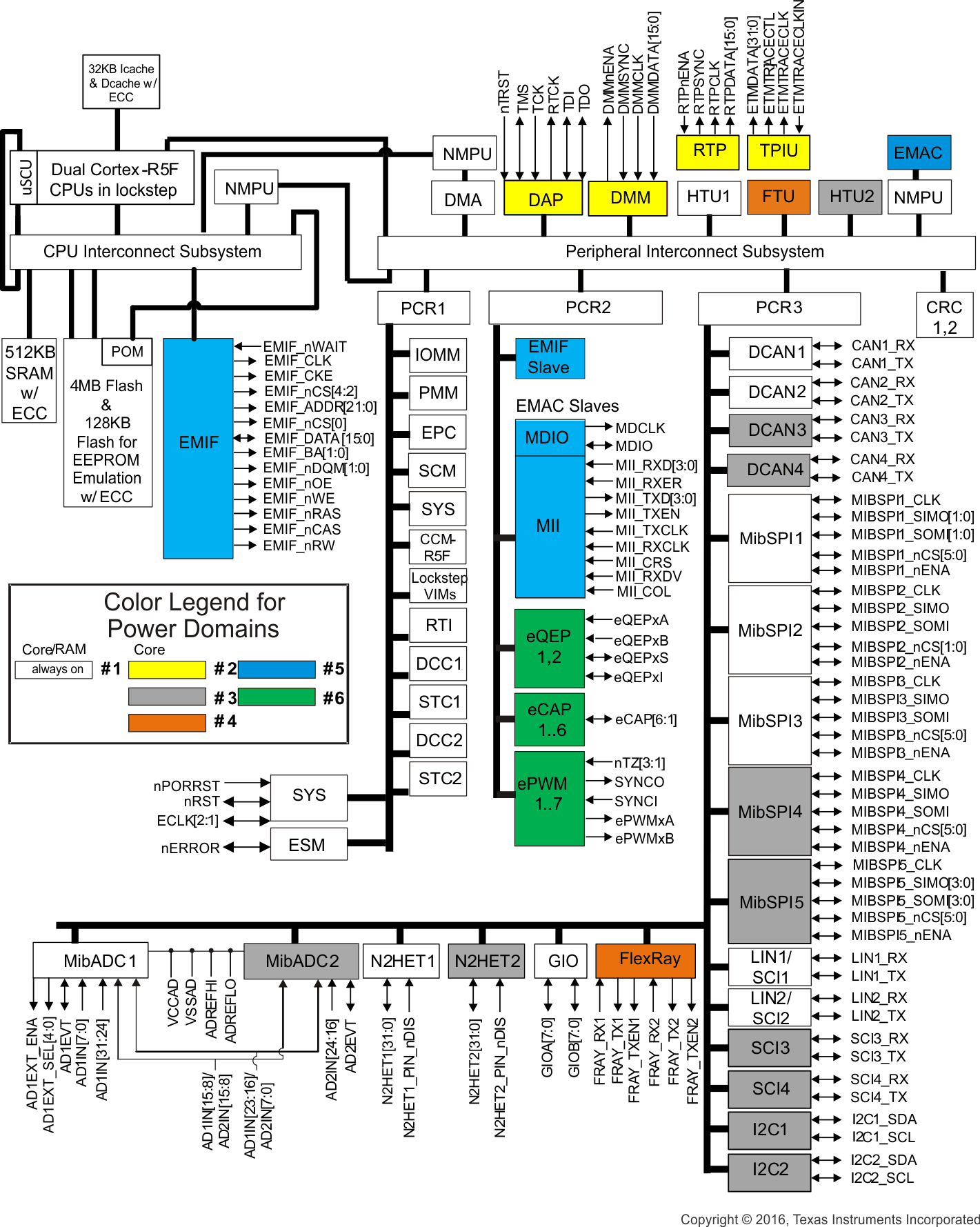
 Figure 2-1 Functional Block Diagram of
the TMS570LC4357-SEP