SPRUJ66A February 2023 – December 2023
- 1
- Abstract
- Trademarks
- 1EVM Revisions and Assembly Variants
- 2Inside the Box
- 3EMC, EMI, and ESD Compliance
-
4System Description
- 4.1 Key Features
- 4.2 Functional Block Diagram
- 4.3 AM62A Low Power SK EVM Interface Mapping
- 4.4 Power ON/OFF Procedures
- 4.5
Peripheral and Major Component Description
- 4.5.1 Clocking
- 4.5.2 Reset
- 4.5.3 CSI Interface
- 4.5.4 Audio Codec Interface
- 4.5.5 HDMI Display Interface
- 4.5.6 JTAG Interface
- 4.5.7 Test Automation Header
- 4.5.8 UART Interface
- 4.5.9 USB Interface
- 4.5.10 Memory Interfaces
- 4.5.11 Ethernet Interface
- 4.5.12 GPIO Port Expander
- 4.5.13 GPIO Mapping
- 4.5.14 Power
- 4.5.15 AM62A Low Power SK EVM User Setup and Configuration
- 4.5.16 Expansion Headers
- 4.5.17 I2C Address Mapping
- 5Revision History
4.5.14.2 Power Input
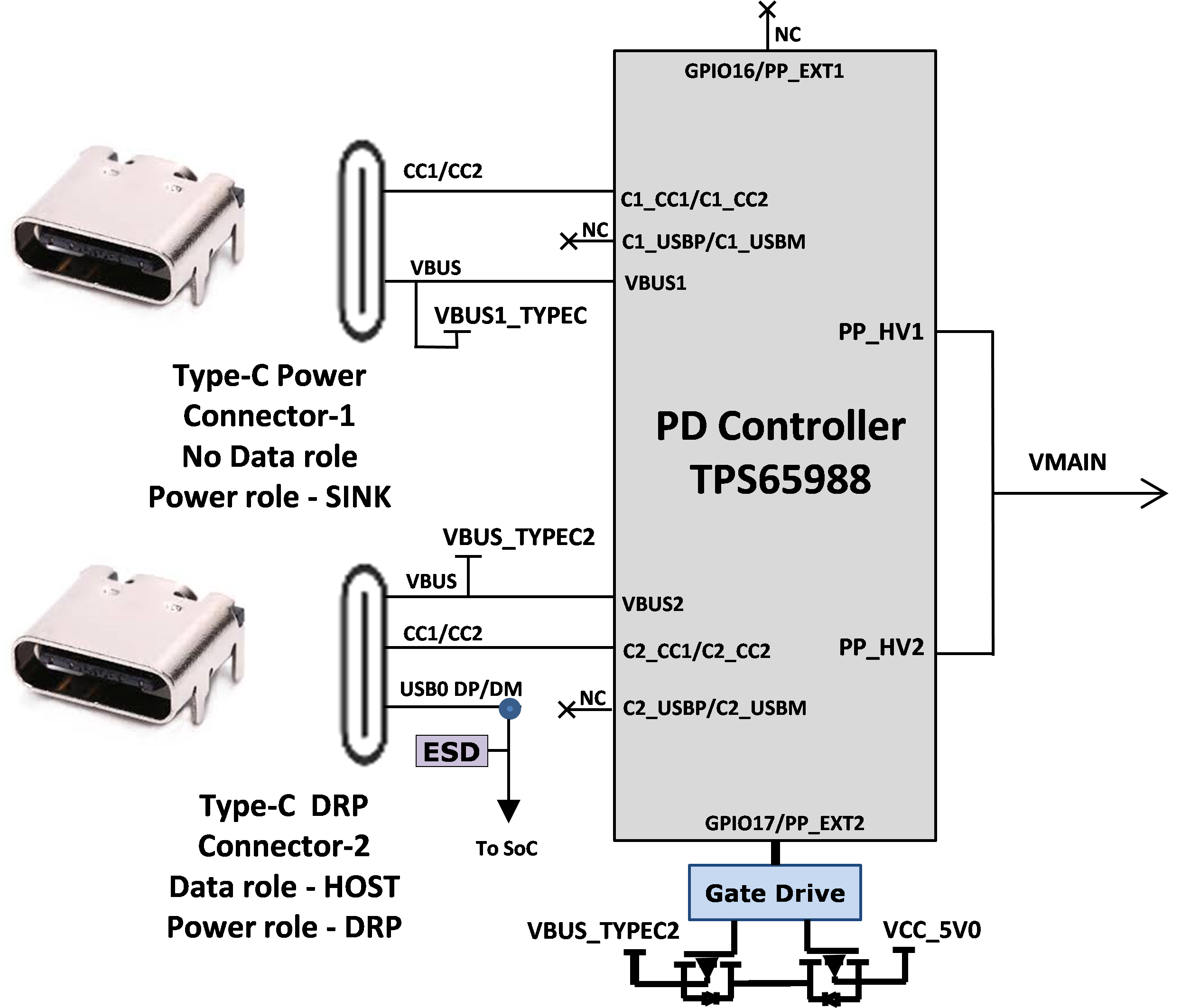
Both Type-C Connectors (VBUS and CC lines) are connected to a Dual PD controller Mfr Part# TPS65988. The TPS65988is a stand-alone USB Type-C and Power Delivery (PD) controller providing cable plug and orientation detection for two USB Type-C Connectors. Upon cable detection, the TPS65988 communicates on the CC wire using the USB PD protocol. When cable detection and USB PD negotiation are complete, the TPS65988 enables the appropriate power path. The two internal power paths of TPS65988 are configured as sink paths for the two Type-C ports and an external FET path is provided for Type-C CONN 2 to source 5V when acting as DFP. The external FET path is controlled by GPIO17/PP_EXT2 of the PD controller along with a resistor option to also enable using USB0 DRVVBUS from AM62A SOC. TPS65988 PD controller can provide an output of 3A (15V max) through CC negotiation. The VBUS pins from both the Type C connectors are connected to the VBUS pins of the PD controller. The output of the PD is VMAIN which is suplied to on board Buck-Boost and Buck regulators to generate fixed 5V and 3.3V supply for the SKEVM board.
 Figure 4-29 Power Input block diagram