SPRUJ67A October 2022 – October 2023
2.1 Functional Block Diagram
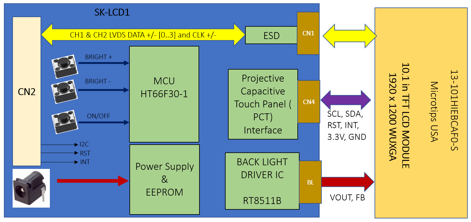
The SK-LCD1 functional block diagram is shown below. The LCD panel is interfaced to adapter board using CN1, CN4 and BL connectors in the adapter board. The EVM is interfaced to LCD kit using CN2 connector on the LCD adapter board.
 Figure 2-3 Functional Block
Diagram